Superconducting Technology Assessment - nitrd
Superconducting Technology Assessment - nitrd
Superconducting Technology Assessment - nitrd

You also want an ePaper? Increase the reach of your titles
YUMPU automatically turns print PDFs into web optimized ePapers that Google loves.
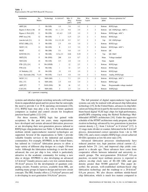
Table 1<br />
Representative Nb and NbN-Based IC Processes<br />
systems and ultrafast digital switching networks will benefit<br />
from its unparalleled speed and low power that far outweighs<br />
the need to provide 4 or 10 K operating environment [10],<br />
[11]. RSFQ logic may play a key role in future quantum<br />
computers as readout and control circuits for Josephson<br />
junction-based qubits [12]–[14].<br />
For these reasons, RSFQ logic has gained wide<br />
acceptance. In the past ten years, many organizations<br />
have developed and sustain advanced fabrication processes<br />
or are developing their next-generation process tailored to<br />
RSFQ logic chip production (see Table 1). Both niobium and<br />
niobium nitride superconductor material technologies are<br />
supported. Several of the organizations in Table 1 provide<br />
valuable foundry services to the industrial and academic<br />
communities. For example, HYPRES, in the United States,<br />
has tailored its 1-kA/cm fabrication process to allow a<br />
large variety of different chip designs on a single 150-mm<br />
wafer. Although the fabrication technology is not the most<br />
advanced, the cost per chip is low, which is particularly<br />
attractive to the academic community for testing a new<br />
idea or design. HYPRES is also developing an advanced<br />
4.5-kA/cm foundry process and a very low current density,<br />
30-A/cm process for the development of quantum computing<br />
circuits. Foundry services, available from SRL, are<br />
enabling many groups in Japan to design and test new circuit<br />
concepts. The SRL foundry offers a 2.5-kA/cm process and<br />
is developing its next-generation 10-kA/cm process.<br />
The full potential of digital superconductor logic-based<br />
systems can only be realized with advanced chip fabrication<br />
technology [15]. In the United States, advances in chip fabrication<br />
are being driven in part by the need to demonstrate niobium-based<br />
digital VLSI logic chips for high-performance,<br />
petaFLOPS computing using the Hybrid <strong>Technology</strong> Multithreaded<br />
(HTMT) architecture [16]. Under the aggressive<br />
schedule of the HTMT architecture study program, chip fabrication<br />
technology advanced by two generations in junction<br />
current density from 2 kA/cm to 8 kA/cm [17]. A<br />
12-stage static divider or counter, fabricated in the 8-kA/cm<br />
process, demonstrated correct operation from dc to 300<br />
GHz [18], and a more complex RSFQ logic circuit achieved<br />
60-Gb/s operation at low bit error rates [19].<br />
Advanced fabrication processes simultaneously have<br />
reduced junction size, kept junction critical current<br />
spreads below 2% 1 , and improved chip yields compared<br />
to a decade ago. These advances have come from<br />
cooperative efforts between industrial and university research<br />
groups. The next-generation 20-kA/cm 0.8- m<br />
junction, six-metal layer niobium process is expected to<br />
achieve on-chip clock rates of 80–100 GHz and gate<br />
density greater than 50 000 gates/cm . This paper describes<br />
the present, well-established niobium-based chip<br />
fabrication technology and the roadmap to a 20-kA/cm<br />
0.8- m process. We also discuss niobium nitride-based<br />
chip fabrication, which is much less mature compared to<br />
1518 PROCEEDINGS OF THE IEEE, VOL. 92, NO. 10, OCTOBER 2004