Superconducting Technology Assessment - nitrd
Superconducting Technology Assessment - nitrd
Superconducting Technology Assessment - nitrd

Create successful ePaper yourself
Turn your PDF publications into a flip-book with our unique Google optimized e-Paper software.
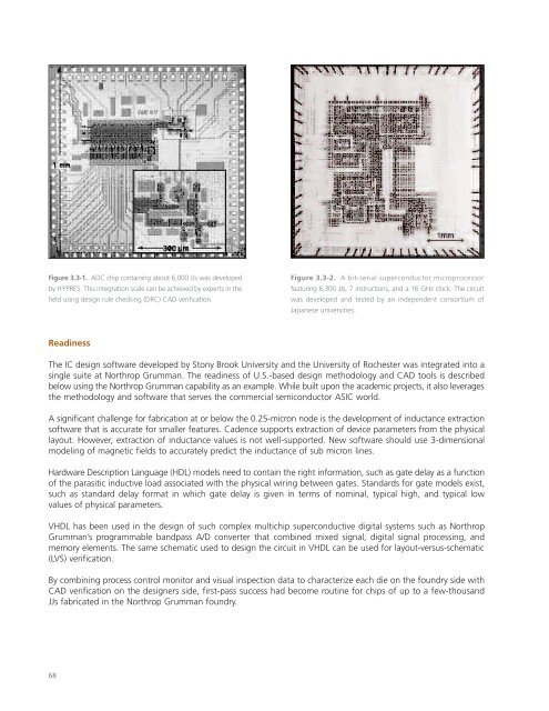
Figure 3.3-1. ADC chip containing about 6,000 JJs was developed<br />
by HYPRES. This integration scale can be achieved by experts in the<br />
field using design rule checking (DRC) CAD verification.<br />
Figure 3.3-2. A bit-serial superconductor microprocessor<br />
featuring 6,300 JJs, 7 instructions, and a 16 GHz clock. The circuit<br />
was developed and tested by an independent consortium of<br />
Japanese universities.<br />
Readiness<br />
The IC design software developed by Stony Brook University and the University of Rochester was integrated into a<br />
single suite at Northrop Grumman. The readiness of U.S.-based design methodology and CAD tools is described<br />
below using the Northrop Grumman capability as an example. While built upon the academic projects, it also leverages<br />
the methodology and software that serves the commercial semiconductor ASIC world.<br />
A significant challenge for fabrication at or below the 0.25-micron node is the development of inductance extraction<br />
software that is accurate for smaller features. Cadence supports extraction of device parameters from the physical<br />
layout. However, extraction of inductance values is not well-supported. New software should use 3-dimensional<br />
modeling of magnetic fields to accurately predict the inductance of sub micron lines.<br />
Hardware Description Language (HDL) models need to contain the right information, such as gate delay as a function<br />
of the parasitic inductive load associated with the physical wiring between gates. Standards for gate models exist,<br />
such as standard delay format in which gate delay is given in terms of nominal, typical high, and typical low<br />
values of physical parameters.<br />
VHDL has been used in the design of such complex multichip superconductive digital systems such as Northrop<br />
Grumman’s programmable bandpass A/D converter that combined mixed signal, digital signal processing, and<br />
memory elements. The same schematic used to design the circuit in VHDL can be used for layout-versus-schematic<br />
(LVS) verification.<br />
By combining process control monitor and visual inspection data to characterize each die on the foundry side with<br />
CAD verification on the designers side, first-pass success had become routine for chips of up to a few-thousand<br />
JJs fabricated in the Northrop Grumman foundry.<br />
68