

1Gb: x8, x16 Automotive DDR2 SDRAM - Micron
1Gb: x8, x16 Automotive DDR2 SDRAM - Micron
1Gb: x8, x16 Automotive DDR2 SDRAM - Micron

Create successful ePaper yourself
Turn your PDF publications into a flip-book with our unique Google optimized e-Paper software.
± tDQSS. tDQSS is specified with a relatively wide range (25% of one clock cycle). All of<br />
the WRITE diagrams show the nominal case, and where the two extreme cases ( tDQSS [MIN] and tDQSS [MAX]) might not be intuitive, they have also been included. Figure 55<br />
(page 101) shows the nominal case and the extremes of tDQSS for BL = 4. Upon completion<br />
of a burst, assuming no other commands have been initiated, the DQ will remain<br />
High-Z and any additional input data will be ignored.<br />
Data for any WRITE burst may be concatenated with a subsequent WRITE command to<br />
provide continuous flow of input data. The first data element from the new burst is applied<br />
after the last element of a completed burst. The new WRITE command should be<br />
issued x cycles after the first WRITE command, where x equals BL/2.<br />
Figure 56 (page 102) shows concatenated bursts of BL = 4 and how full-speed random<br />
write accesses within a page or pages can be performed. An example of nonconsecutive<br />
WRITEs is shown in Figure 57 (page 102). <strong>DDR2</strong> <strong>SDRAM</strong> supports concurrent auto precharge<br />
options, as shown in Table 42.<br />
<strong>DDR2</strong> <strong>SDRAM</strong> does not allow interrupting or truncating any WRITE burst using BL = 4<br />
operation. Once the BL = 4 WRITE command is registered, it must be allowed to complete<br />
the entire WRITE burst cycle. However, a WRITE BL = 8 operation (with auto precharge<br />
disabled) might be interrupted and truncated only by another WRITE burst as<br />
long as the interruption occurs on a 4-bit boundary due to the 4n-prefetch architecture<br />
of <strong>DDR2</strong> <strong>SDRAM</strong>. WRITE burst BL = 8 operations may not be interrupted or truncated<br />
with any command except another WRITE command, as shown in Figure 58<br />
(page 103).<br />
Data for any WRITE burst may be followed by a subsequent READ command. To follow<br />
a WRITE, tWTR should be met, as shown in Figure 59 (page 104). The number of clock<br />
cycles required to meet tWTR is either 2 or tWTR/ tCK, whichever is greater. Data for any<br />
WRITE burst may be followed by a subsequent PRECHARGE command. tWR must be<br />
met, as shown in Figure 60 (page 105). tWR starts at the end of the data burst, regardless<br />
of the data mask condition.<br />
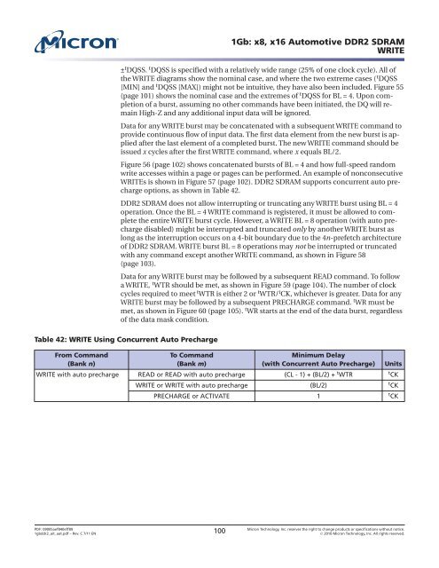
Table 42: WRITE Using Concurrent Auto Precharge<br />
From Command<br />
(Bank n)<br />
To Command<br />
(Bank m)<br />
<strong>1Gb</strong>: <strong>x8</strong>, <strong>x16</strong> <strong>Automotive</strong> <strong>DDR2</strong> <strong>SDRAM</strong><br />
WRITE<br />
Minimum Delay<br />
(with Concurrent Auto Precharge) Units<br />
WRITE with auto precharge READ or READ with auto precharge (CL - 1) + (BL/2) + tWTR tCK WRITE or WRITE with auto precharge (BL/2) tCK PRECHARGE or ACTIVATE 1 tCK PDF: 09005aef840eff89<br />
1gbddr2_ait_aat.pdf – Rev. C 7/11 EN 100 <strong>Micron</strong> Technology, Inc. reserves the right to change products or specifications without notice.<br />
� 2010 <strong>Micron</strong> Technology, Inc. All rights reserved.


