

1Gb: x8, x16 Automotive DDR2 SDRAM - Micron
1Gb: x8, x16 Automotive DDR2 SDRAM - Micron
1Gb: x8, x16 Automotive DDR2 SDRAM - Micron

You also want an ePaper? Increase the reach of your titles
YUMPU automatically turns print PDFs into web optimized ePapers that Google loves.
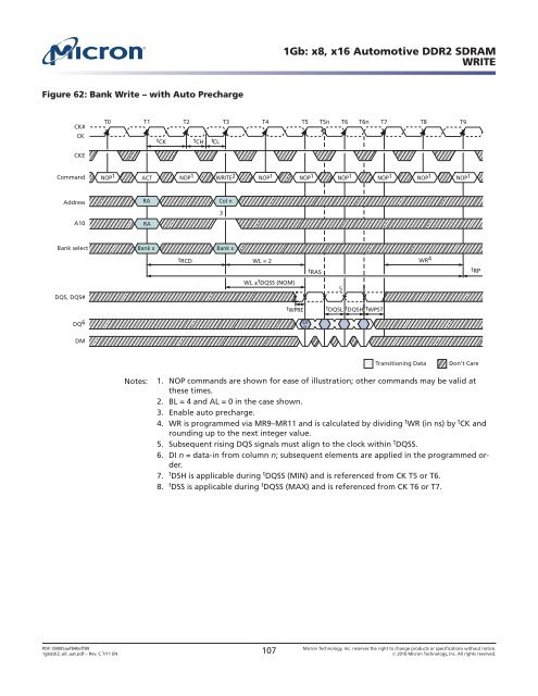
Figure 62: Bank Write – with Auto Precharge<br />
CK#<br />
CK<br />
CKE<br />
Command<br />
Address<br />
A10<br />
Bank select<br />
DQS, DQS#<br />
DQ 6<br />
DM<br />
T0 T1 T2 T3 T4 T5 T5n T6 T6n T7 T8<br />
NOP 1<br />
ACT<br />
RA<br />
tCK tCH tCL<br />
NOP 1<br />
RA Col n<br />
Bank x<br />
tRCD<br />
WRITE2 NOP1 NOP1 NOP1 NOP1 NOP1 3<br />
Bank x<br />
WL = 2<br />
WL ±tDQSS (NOM)<br />
<strong>1Gb</strong>: <strong>x8</strong>, <strong>x16</strong> <strong>Automotive</strong> <strong>DDR2</strong> <strong>SDRAM</strong><br />
WRITE<br />
tWPRE<br />
DI<br />
n<br />
tRAS<br />
5<br />
tDQSL tDQSH tWPST<br />
WR 4<br />
Transitioning Data<br />
T9<br />
NOP 1<br />
tRP<br />
Don’t Care<br />
Notes: 1. NOP commands are shown for ease of illustration; other commands may be valid at<br />
these times.<br />
2. BL = 4 and AL = 0 in the case shown.<br />
3. Enable auto precharge.<br />
4. WR is programmed via MR9–MR11 and is calculated by dividing t WR (in ns) by t CK and<br />
rounding up to the next integer value.<br />
5. Subsequent rising DQS signals must align to the clock within t DQSS.<br />
6. DI n = data-in from column n; subsequent elements are applied in the programmed order.<br />
7. t DSH is applicable during t DQSS (MIN) and is referenced from CK T5 or T6.<br />
8. t DSS is applicable during t DQSS (MAX) and is referenced from CK T6 or T7.<br />
PDF: 09005aef840eff89<br />
1gbddr2_ait_aat.pdf – Rev. C 7/11 EN 107 <strong>Micron</strong> Technology, Inc. reserves the right to change products or specifications without notice.<br />
� 2010 <strong>Micron</strong> Technology, Inc. All rights reserved.


