- Page 1 and 2:
Automotive DDR2 SDRAM MT47H128M8 -
- Page 3 and 4:
1Gb: x8, x16 Automotive DDR2 SDRAM
- Page 5 and 6:
1Gb: x8, x16 Automotive DDR2 SDRAM
- Page 7 and 8:
1Gb: x8, x16 Automotive DDR2 SDRAM
- Page 9 and 10:
Functional Description Automotive I
- Page 11 and 12:
Functional Block Diagrams The DDR2
- Page 13 and 14:
Ball Assignments and Descriptions F
- Page 15 and 16:
Table 3: FBGA 84-Ball - x16 and 60-
- Page 17 and 18:
Packaging Package Dimensions Figure
- Page 19 and 20:
FBGA Package Capacitance Table 4: I
- Page 21 and 22:
Table 6: Temperature Limits Paramet
- Page 23 and 24:
I DD7 Conditions The detailed timin
- Page 25 and 26:
Table 10: DDR2 I DD Specifications
- Page 27 and 28:
PDF: 09005aef840eff89 Micron Techno
- Page 29 and 30:
PDF: 09005aef840eff89 Micron Techno
- Page 31 and 32:
PDF: 09005aef840eff89 Micron Techno
- Page 33 and 34:
PDF: 09005aef840eff89 Micron Techno
- Page 35 and 36:
PDF: 09005aef840eff89 Micron Techno
- Page 37 and 38:
PDF: 09005aef840eff89 Micron Techno
- Page 39 and 40:
AC and DC Operating Conditions Tabl
- Page 41 and 42:
Input Electrical Characteristics an
- Page 43 and 44:
1Gb: x8, x16 Automotive DDR2 SDRAM
- Page 45 and 46:
Table 19: Output Characteristics Pa
- Page 47 and 48:
Figure 15: Full Strength Pull-Up Ch
- Page 49 and 50:
Figure 17: Reduced Strength Pull-Up
- Page 51 and 52:
AC Overshoot/Undershoot Specificati
- Page 53 and 54:
Input Slew Rate Derating 1Gb: x8, x
- Page 55 and 56:
1Gb: x8, x16 Automotive DDR2 SDRAM
- Page 57 and 58:
Figure 23: Nominal Slew Rate for t
- Page 59 and 60:
1Gb: x8, x16 Automotive DDR2 SDRAM
- Page 61 and 62:
Table 34: Single-Ended DQS Slew Rat
- Page 63 and 64:
Figure 27: Nominal Slew Rate for t
- Page 65 and 66:
Figure 31: AC Input Test Signal Wav
- Page 67 and 68:
6. Bank addresses (BA) determine wh
- Page 69 and 70:
Table 38: Truth Table - Current Sta
- Page 71 and 72:
NO OPERATION (NOP) LOAD MODE (LM) A
- Page 73 and 74:
Burst Length Figure 33: MR Definiti
- Page 75 and 76: Write Recovery Power-Down Mode 1Gb:
- Page 77 and 78: Extended Mode Register (EMR) Figure
- Page 79 and 80: On-Die Termination (ODT) ODT effect
- Page 81 and 82: Extended Mode Register 2 (EMR2) Fig
- Page 83 and 84: PDF: 09005aef840eff89 Micron Techno
- Page 85 and 86: 1Gb: x8, x16 Automotive DDR2 SDRAM
- Page 87 and 88: Figure 42: Multibank Activate Restr
- Page 89 and 90: Figure 43: READ Latency CK# CK Comm
- Page 91 and 92: Figure 45: Nonconsecutive READ Burs
- Page 93 and 94: Figure 48: READ-to-PRECHARGE - BL =
- Page 95 and 96: Figure 50: Bank Read - Without Auto
- Page 97 and 98: Figure 52: x4, x8 Data Output Timin
- Page 99 and 100: Figure 54: Data Output Timing - t A
- Page 101 and 102: Figure 55: Write Burst CK# CK Comma
- Page 103 and 104: Figure 58: WRITE Interrupted by WRI
- Page 105 and 106: Figure 60: WRITE-to-PRECHARGE CK# C
- Page 107 and 108: Figure 62: Bank Write - with Auto P
- Page 109 and 110: Figure 64: Data Input Timing PRECHA
- Page 111 and 112: SELF REFRESH 1Gb: x8, x16 Automotiv
- Page 113 and 114: Power-Down Mode 1Gb: x8, x16 Automo
- Page 115 and 116: Table 43: Truth Table - CKE 1Gb: x8
- Page 117 and 118: Figure 70: WRITE-to-Power-Down or S
- Page 119 and 120: Figure 74: PRECHARGE Command-to-Pow
- Page 121 and 122: Reset CKE Low Anytime 1Gb: x8, x16
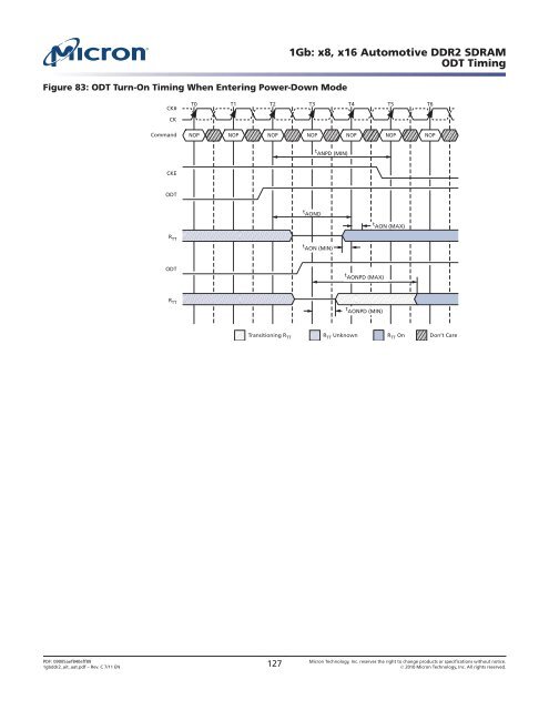
- Page 123 and 124: ODT Timing 1Gb: x8, x16 Automotive
- Page 125: MRS Command to ODT Update Delay Dur
- Page 129: Figure 85: ODT Turn-On Timing When