

1Gb: x8, x16 Automotive DDR2 SDRAM - Micron
1Gb: x8, x16 Automotive DDR2 SDRAM - Micron
1Gb: x8, x16 Automotive DDR2 SDRAM - Micron

You also want an ePaper? Increase the reach of your titles
YUMPU automatically turns print PDFs into web optimized ePapers that Google loves.
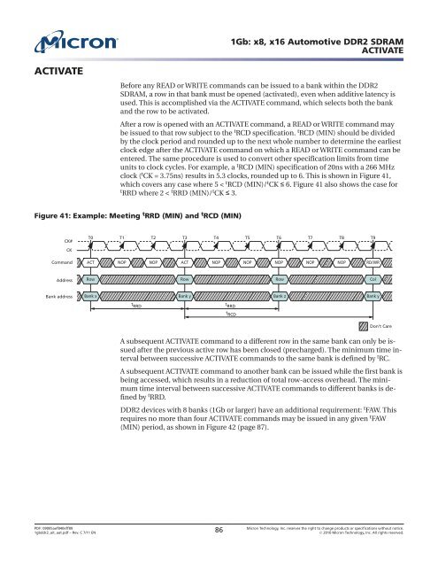
ACTIVATE<br />
Before any READ or WRITE commands can be issued to a bank within the <strong>DDR2</strong><br />
<strong>SDRAM</strong>, a row in that bank must be opened (activated), even when additive latency is<br />
used. This is accomplished via the ACTIVATE command, which selects both the bank<br />
and the row to be activated.<br />
After a row is opened with an ACTIVATE command, a READ or WRITE command may<br />
be issued to that row subject to the tRCD specification. tRCD (MIN) should be divided<br />
by the clock period and rounded up to the next whole number to determine the earliest<br />
clock edge after the ACTIVATE command on which a READ or WRITE command can be<br />
entered. The same procedure is used to convert other specification limits from time<br />
units to clock cycles. For example, a tRCD (MIN) specification of 20ns with a 266 MHz<br />
clock ( tCK = 3.75ns) results in 5.3 clocks, rounded up to 6. This is shown in Figure 41,<br />
which covers any case where 5 < tRCD (MIN)/ tCK ≤ 6. Figure 41 also shows the case for<br />
tRRD where 2 < tRRD (MIN)/ tCK ≤ 3.<br />
Figure 41: Example: Meeting t RRD (MIN) and t RCD (MIN)<br />
CK#<br />
CK<br />
Command<br />
Address<br />
Bank address<br />
T0 T1<br />
T2 T3 T4 T5 T6 T7<br />
ACT NOP<br />
NOP ACT NOP<br />
NOP NOP NOP NOP<br />
RD/WR<br />
Row Row Row<br />
Col<br />
Bank x Bank y<br />
t RRD<br />
t RRD<br />
<strong>1Gb</strong>: <strong>x8</strong>, <strong>x16</strong> <strong>Automotive</strong> <strong>DDR2</strong> <strong>SDRAM</strong><br />
ACTIVATE<br />
t RCD<br />
T8 T9<br />
Bank z Bank y<br />
Don’t Care<br />
A subsequent ACTIVATE command to a different row in the same bank can only be issued<br />
after the previous active row has been closed (precharged). The minimum time interval<br />
between successive ACTIVATE commands to the same bank is defined by tRC. A subsequent ACTIVATE command to another bank can be issued while the first bank is<br />
being accessed, which results in a reduction of total row-access overhead. The minimum<br />
time interval between successive ACTIVATE commands to different banks is defined<br />
by tRRD. <strong>DDR2</strong> devices with 8 banks (<strong>1Gb</strong> or larger) have an additional requirement: tFAW. This<br />
requires no more than four ACTIVATE commands may be issued in any given tFAW (MIN) period, as shown in Figure 42 (page 87).<br />
PDF: 09005aef840eff89<br />
1gbddr2_ait_aat.pdf – Rev. C 7/11 EN 86 <strong>Micron</strong> Technology, Inc. reserves the right to change products or specifications without notice.<br />
� 2010 <strong>Micron</strong> Technology, Inc. All rights reserved.


