areorient themselves with the electric field., mer are isrefractive the internal index incident <strong>of</strong> theangle EO polymer, <strong>of</strong> the light and _After poling another glass slide with ITOhlymer<strong>of</strong> going is thethrough internalthe incident device.The<strong>of</strong> waves the light inand DBR is placed on top <strong>of</strong> the EOe, ch a<strong>of</strong>phase goingare through reinforced ELECTRO-OPTIC the device. through PROPERTIES The constructive waves OF HYBRID in SOL-GEL MATERIALS IN FABRY-PEROT MODULATORSpolymer and electrical wires are connectedte, d a a interference, phase are reinforced resultingthrough strong constructive narrowWhere λ is the wavelength <strong>of</strong> the incident wave, l is the with the electric to each field. ITO After layer. poling another The layers glass slide are with thenITOuted and a transmission interference, bands resulting that in vary strong depending narrowthickness <strong>of</strong> the film, n is the refractive index <strong>of</strong> the EO polymer, and DBR is clamped placed on top and<strong>of</strong> epoxy the EO is polymer applied and to electrical seal the wiresbuted ror. upon transmission the multiple bands factors that varyshown dependingand θ is the internal incident angle <strong>of</strong> the light going through the are connected device. to each ITO layer. The layers are then clamped andirror. upon the ). multiple They factors include filmindevice. The waves in phase are reinforced through constructive epoxy is applied to seal the device.thickness, change ). in refractive They include index due filminterference, resulting in strong narrow transmission bands thattothickness, EO effect, change and surface in refractive roughness. index In duevary depending upon the multiple factors shown in Equation (1).general to EO transmission effect, and surface will occur roughness. wheneverInThey include film thickness, change in refractive index due to the general phasetransmission shift satisfies will the occur following wheneverEO effect, and surface roughness. In general transmission will equation: the phase shift satisfies the followingSol-gel filmoccur wheneverequation:the phase shift satisfies the following equation: ; ;where m = any integer where m = any integer Equation 2. where m = any integerA typical wavelength versusA typical transmission wavelength Aspectra versus typical transmission illustrating wavelength spectra thisillustratingversusthis is shown transmission in in Figure 3.below. illustrating this isshown in change below.change in in the the piezo piezo (mechanical) forces acting acting upon upon the the material.Figure 4. Corona Poling Apparatusd inThe resonance wavelength and thesed s asinshift in in that wavelength are measured byusing a broadband METHODSsource which outputsons ticalasIndium Indiumtintin oxide, oxide, a a transparentthrough a fiber collimator into the Fabry-The resonance wavelength and the shift in that wavelengthptical theconductive conductive material material acts acts as asthe theelectrode electrodeininPerot Perot Etalon.Light that is transmittedthethedevicedeviceandandisisthethefirstfirstlayerlayerdepositeddepositedh theare measured fromfromthetheby cavitycavity using isisfocused a broadband ontoonto asourcesinglesingle which outputsontoontothetheglassglasssubstrate.substrate.ThenThenthetheDBRDBRthrough modemodea fiber fiberfibercollimator detectordetectorinto whichwhich leadsthe Fabry-Perot leadstoto aEtalon. Light thatthelayerlayerisiscoatedcoatedonontoptopfollowedfollowedbybythetheopticalopticalspectrumspectrumanalyzeranalyzer (OSA).(OSA).TheTheTCBD sol-gel. The TCBD sol-gel isde thetransmitted from the cavity is focused onto a single mode fiberghlyTCBD sol-gel. The TCBD sol-gel is OSA measures the wavelength while theprepared and spin coated at varying speedsOSA measures the wavelength while theighlyprepared and spin coated at varying speedsdetector applied which leads voltage to a is optical varied spectrum letting analyzer the (OSA). Thenceto set the thickness <strong>of</strong> the EO polymerapplied voltage is varied letting theto set the thickness <strong>of</strong> the EO polymerwavelength shift be directly observed.renceOSA measures the wavelength while the applied voltage is variedonlyfilm. After baking, this layered material is wavelength shift be directly observed.film. After baking, this layered material isBy switching the broadband source to corona poled above the glass transition By switching the broadband source to aonlyletting the narrowband, wavelength tunable shift be laser directly the extinction observed.eingcoronatemperaturepoledatabovea highthevoltage.glass transitionPoling is narrowband,beingBy ratio switching and the dynamictunablebroadband modulationlaser the extinctionsource to <strong>of</strong>a the narrowband, tunablewilltemperaturedone to orientat athehighchromophorevoltage. Polingmoleculesis ratiosampleandcandynamicbe measured.modulationThe<strong>of</strong>laserthes will Figure 3. Typical Transmittance done Spectra Fabry Perot Etalon laser the extinction ratio and dynamic modulation <strong>of</strong> the sample<strong>of</strong>andt<strong>of</strong>orceorientnon-centro-symmetrythe chromophore moleculesin the sample propagates canthrough be measured.collimator, The continues laserAdapted from Lambda and film. Research force The Optics non-centro-symmetry combination Inc. <strong>of</strong> temperatures in thee <strong>of</strong>can be measured.propagates through thethrough The device laseracavity collimator,propagates and finally continuesthrough the a collimator, continuesthroughthefilm. above The thecombination glass transition <strong>of</strong> temperatures temperature, throughet in thetransmitted thethe devicelight device iscavityfocused cavity andandont<strong>of</strong>inally finallythe fiber theabove the transmitted lightWhen whichthe causes glass thetransition Si/SiO2 sol temperature, gel matrix to transmitted detector. The light dynamic is focused modulation onto the can fibervoltage is applied to the material a shift in the resonancewavelength occurs and relax, correlates to the change in refrac-are theinwhich is focused onto the fiber detector. The dynamic modulation can relax, causes and the theapplication Si/SiO2 sol <strong>of</strong> gel a high matrix electric to detector. observedThe by dynamic switchingmodulation the DC voltage can beirror s theAdapted from Lambda fieldand Research causes the applicationOptics Inc. the highly <strong>of</strong> a high polarizable electricbe observed observed source by to switching byAC switching by the inserting DC thevoltage DC a function voltage source to AC by insert-a functionfieldtive index (∆n) due Adapted to the from electro-optic chromophore causes theLambda Research effect molecules highlyOptics and Inc. the change topolarizablerotate in and source generator and ACchanging by inserting to a photo a function detectorions irrorchromophore orient themselves molecules with the to electric rotate field. andinggeneratorgenerator and changing to a photo detector whichwhich inputs and changing into a digital to a photo oscilloscope. detectorthickness (∆l) due to a change in the piezo (mechanical) forcesctions When voltage is applied orient After to themselves poling material another withglass the a electric slide with field. ITOinputs into which Seea digital inputs oscilloscope. into a digital below See oscilloscope. for Figures testing5, 6, and 7 belowacting shift upon When in the the voltage material. resonance is applied After wavelength andpoling DBR to the another is material placed occurs glass onaslide top <strong>of</strong> with theITOEOfor testing See schematics. below for testingand shift correlates in the resonance and polymerto the change wavelength DBR and is placed electricalin refractive occurs onwires top are <strong>of</strong> connected the EO schematics.polymer to eachand ITOelectrical layer. wires The layers are connected are then index and DEVICE correlates () due ASSEMBLY to to the toelectro-optic clampedchangeeach ITO / and POLING inlayer.refractiveepoxy effect The is applied layerstoare seal thenindex () due to the electro-optic effect Indium and the tin change oxide, a in transparent thickness clamped device. andconductive () epoxy due material to is applied a to seal theacts asand the change in thickness device. () due to athe electrode in the device and is the first layer deposited onto the glass substrate. Then the DBR layeris coated on top followed by the TCBD sol-gel. The TCBD sol-gel is prepared and spin coated 1 No. 1 at Summer varying 2004 speeds to set the thickness Sol-gel <strong>of</strong> filmthe EO polymer film. AfterSummer baking, 2004 this layered material Sol-gel is corona film poled above the glassFigure 5. Shift Measurement Schematicol. 1 No. 1 transition temperature at a high voltage. Poling is done to orient the chromophore molecules and force non-centro-symmetry inthe film. The combination <strong>of</strong> temperatures abovethe glass transitiontemperature, which causes the Si/SiO 2 sol gel matrix to relax, and the application <strong>of</strong> a high electric field causes the highly polarizablechromophore molecules to rotate and orient themselves Figure 6. Extinction Measurement Schematic36 CMDITR Review <strong>of</strong> Undergraduate Research Vol. 2 No. 1 Summer <strong>2005</strong>CMDITR Review <strong>of</strong> Undergraduate Research Vol. 1 No. 1 Summer 2004 whiSeeschCMDITR Review <strong>of</strong> Undergrad
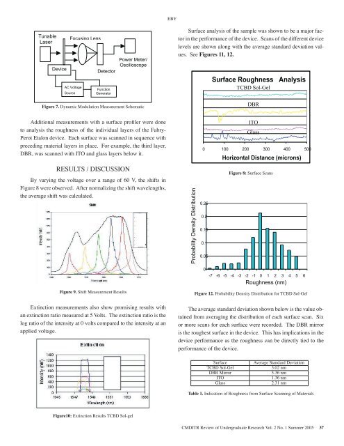
facethef therfaceding, theITOthird layer, DBR, was scanned with ITOand glass layers below it. Additional measurements with a surfacepr<strong>of</strong>iler were done to analysis theroughness Figure 7. Dynamic <strong>of</strong> the Modulation individual Measurement layers Schematic <strong>of</strong> theFabry-Perot Etalon device. Each surfaceAdditional was scanned measurements in sequence with a surface with preceding pr<strong>of</strong>iler were donematerial layers in place. For example, theto analysisthirdthelayer,roughnessDBR,<strong>of</strong>wasthe individualscannedlayerswith<strong>of</strong>ITOthe Fabry-Perot Etalon and glass device. layers Each below surface it. was scanned in sequence withAdditional measurements with a surfacepreceding material layers in place. For example, the third layer,pr<strong>of</strong>ilerDBR, were done to analysis thewas scanned with ITO and glass layers below it.roughness By varying<strong>of</strong> the the voltage individual over alayers range<strong>of</strong> <strong>of</strong>the60Fabry-Perot V, the shiftsEtalon in device. were Each observed. surfacewas Afterscanned normalizing RESULTSin sequence/ the DISCUSSION shift with wavelengths, precedingBythevaryingaveragetheshiftvoltagewasovercalculated.material layers in place. a range For example, <strong>of</strong> 60 V, the the shifts inFigure third 8 were layer, observed. DBR, After was normalizing scanned the with shift wavelengths, ITOthe average shift was calculated.and glass layers below it.By varying the voltage over a range <strong>of</strong> 60V, the shifts in were observed.After normalizing the shift wavelengths,the average shift was calculated.ExtinctionFigure measurements 9. Shift Measurement Results also showpromising results with an extinction ratioExtinction measured measurements at 5 Volts. also The show extinction promising ratio results withan extinction is theratio logmeasured ratio <strong>of</strong>at the 5 Volts. intensity The extinction at 0 volts ratio is thelog ratio compared <strong>of</strong> the intensity to the at 0 volts intensity compared at to anthe applied intensity at anapplied voltage.4 CMDITR Review <strong>of</strong> Undergraduate Research Vol. 1 No. 1 Summer 20044 CMDITR Review <strong>of</strong> Undergraduate Research Vol. 1 No. 1 Summer 2004Figure10: Extinction Results TCBD Sol-gelExtinction measurements also showEBY promising results with an extinction ratiomeasured at 5 Volts. The extinction ratiois the Surface log ratio analysis <strong>of</strong> the <strong>of</strong> the intensity sample was at shown 0 volts to be a major factorin the performance <strong>of</strong> the device. Scans <strong>of</strong> the different deviceExtinction compared tomeasurements the intensity atalso an applied showpromising voltage.levels are results with an extinction ratioshown along with the average standard deviation values.See Figures 11,measured at 5 Volts. The extinction ratio12.By varying the voltage over a range <strong>of</strong> 60V, the shifts in were observed.After normalizing the shift wavelengths,the average shift was calculated. is the log Surface ratioanalysis <strong>of</strong> the intensity <strong>of</strong> the sample at 0 volts was showncompared to beto a the major intensity factor inat the an performance applied <strong>of</strong>voltage.DBRSurface analysis <strong>of</strong> the sample ITOwas shownto be a major factor in the performance <strong>of</strong>the device. Scans <strong>of</strong> the different Glass devicelevels are shown along with the averagestandard deviation values. See Surfacethe analysis device. <strong>of</strong> Scans the Figure sample 8: <strong>of</strong>Surface the was Scans different shown deviceto be alevels major are factor shown in thealong performance with the<strong>of</strong>averagethe device. standard Scans deviation <strong>of</strong> the different values. device See levels are shown along with the averageTCBD Sol-Gelstandard deviation values. See DBR 4 CMDITR Review <strong>of</strong> Undergraduate Research Vol. 1 No. 1 Summer 2004 ITOGlassSurface analysis <strong>of</strong> the sample was shownto be a major factor in the performance <strong>of</strong>TCBD Sol-Gel DBRFigure 12. Probability Density Distribution for TCBD Sol-Gel standard ITOThe average standard deviation shown deviation below is shown the value obtainedfrom averaging Glassbelow is thethe distributionvalue obtained<strong>of</strong> each surfacefromscan. Sixor more scans for each surface were recorded. The DBR mirroraveraging the distribution <strong>of</strong> each surfaceis the roughest surface in the device. This has implications in thescan. Six or more scans for each surfacedevice performance as the roughness can be directly tied to thewereperformancerecorded. The DBR mirror is the<strong>of</strong> the device.roughest surface in the device. This hasimplications in the device performance asthe roughness can be directly tied to theperformance <strong>of</strong> the device.SurfaceTCBD Sol-GelDBR MirrorITOGlassTCBD Sol-GelAverage Standard Deviation3.02 nm5.36 nm1.36 nm2.31 nm Table 1. Indication <strong>of</strong> Roughness from Surface Scanning <strong>of</strong> MaterialsCMDITR Review <strong>of</strong> Undergraduate Research Vol. 2 No. 1 Summer <strong>2005</strong> 37avperPeITImmapuper1.Un2.Jou3.AnLig4.M.Jen15NaUnCo
- Page 2 and 3: The material is based upon work sup
- Page 4 and 5: TABLE OF CONTENTSSynthesis of Dendr
- Page 6 and 7: 6 CMDITR Review of Undergraduate Re
- Page 8 and 9: SYNTHESIS OF DENDRIMER BUILDING BLO
- Page 10 and 11: throughout the work period. Five su
- Page 12 and 13: 12 CMDITR Review of Undergraduate R
- Page 14 and 15: BARIUM TITANATE DOPED SOL-GEL FOR E
- Page 16 and 17: BARIUM TITANATE DOPED SOL-GEL FOR E
- Page 18 and 19: SYNTHESIS OF NORBORNENE MONOMER OF
- Page 20: 20 CMDITR Review of Undergraduate R
- Page 23 and 24: using different reaction conditions
- Page 25 and 26: Synthesis of Nonlinear Optical-Acti
- Page 27 and 28: quality of the XRD structures wasca
- Page 29 and 30: Behavioral Properties of Colloidal
- Page 32 and 33: Transmission electron microscopy ha
- Page 34 and 35: 34 CMDITR Review of Undergraduate R
- Page 38 and 39: Fabry-Perot modulators with electro
- Page 40 and 41: 40 CMDITR Review of Undergraduate R
- Page 42 and 43: QUANTIZED HAMILTON DYNAMICS APPLIED
- Page 44 and 45: 44 CMDITR Review of Undergraduate R
- Page 46 and 47: INVESTIGATING NEW CLADDING AND CORE
- Page 48 and 49: Dr. Robert NorwoodChris DeRoseAmir
- Page 50 and 51: SYNTHESIS OF TPD-BASED COMPOUNDS FO
- Page 52 and 53: SYNTHESIS OF TPD-BASED COMPOUNDS FO
- Page 54 and 55: OPTIMIZING HYBRID WAVEGUIDESpropaga
- Page 56 and 57: At closer spaces the second undesir
- Page 58 and 59: SYNTHESIS AND ANALYSIS OF THIOL-STA
- Page 60 and 61: 60 CMDITR Review of Undergraduate R
- Page 62 and 63: QUINOXALINE-CONTAINING POLYFLUORENE
- Page 64 and 65: QUINOXALINE-CONTAINING POLYFLUORENE
- Page 66 and 67: 66 CMDITR Review of Undergraduate R
- Page 68 and 69: SYNTHESIS OF DENDRON-FUNCTIONALIZED
- Page 70 and 71: 70 CMDITR Review of Undergraduate R
- Page 72 and 73: BUILDING AN OPTICAL OXIMETER TO MEA
- Page 74 and 75: 74 CMDITR Review of Undergraduate R
- Page 76 and 77: 76 CMDITR Review of Undergraduate R
- Page 78 and 79: TOWARD MOLECULAR RESOLUTION C-AFM W
- Page 80 and 81: TOWARD MOLECULAR RESOLUTION C-AFM W
- Page 82 and 83: SYNTHESIS AND CHARACTERIZATION OF E
- Page 84 and 85: My name is Aaron Montgomery and I a
- Page 86 and 87:
1,1-DIPHENYL-2,3,4,5-TETRAKIS(9,9-D
- Page 88 and 89:
1,1-DIPHENYL-2,3,4,5-TETRAKIS(9,9-D
- Page 90 and 91:
EFFECTS OF SURFACE CHEMISTRY ON CAD
- Page 92 and 93:
EFFECTS OF SURFACE CHEMISTRY ON CAD
- Page 94 and 95:
94 CMDITR Review of Undergraduate R
- Page 96 and 97:
SYNTHESIS OF A POLYENE EO CHROMOPHO
- Page 98 and 99:
SYNTHESIS OF A POLYENE EO CHROMOPHO
- Page 102 and 103:
102 CMDITR Review of Undergraduate
- Page 104 and 105:
CHARACTERIZATION OF THE MOLECULAR P
- Page 106 and 107:
106 CMDITR Review of Undergraduate
- Page 108 and 109:
OPTIMIZATION OF SEMICONDUCTOR NANOP
- Page 110 and 111:
OPTIMIZATION OF SEMICONDUCTOR NANOP
- Page 112 and 113:
CHARACTERIZATION OF THE PHOTODECOMP
- Page 114 and 115:
114 CMDITR Review of Undergraduate
- Page 116 and 117:
ELECTROLUMINESCENT PROPERTIES OF OR
- Page 118 and 119:
118 CMDITR Review of Undergraduate
- Page 120 and 121:
DETERMINATION OF MOLECULAR ORIENTAT
- Page 122 and 123:
DETERMINATION OF MOLECULAR ORIENTAT
- Page 124 and 125:
HYDROGEL MATERIALS FOR TWO-PHOTON M
- Page 126 and 127:
HYDROGEL MATERIALS FOR TWO-PHOTON M
- Page 128 and 129:
THE DESIGN OF A FLUID DELIVERY SYST
- Page 130:
THE DESIGN OF A FLUID DELIVERY SYST