Student Project Abstracts 2005 - Pluto - University of Washington
Student Project Abstracts 2005 - Pluto - University of Washington
Student Project Abstracts 2005 - Pluto - University of Washington

Create successful ePaper yourself
Turn your PDF publications into a flip-book with our unique Google optimized e-Paper software.
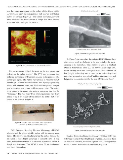
TOWARD MOLECULAR RESOLUTION C-AFM WITH CARBON NANOTUBE TIPS: DEVELOPMENT OF CARBON NANOTUBE GROWTH TECHNIQUESand they were spun-coated on the surface <strong>of</strong> the silicon nitride.AFM images show the nanoparticles had an even distributionacross the surface (Figure 2). The carbon nanotubes grown onthese surfaces were very difficult to image with AFM becausesome soot was forming on the surface.Figure 4: FESEM image <strong>of</strong> a carbon nanotubeFigure 2. Iron nanoparticles on silicon nitride surfaceThe last technique utilized ferrocene as the iron source, andxylenes as the carbon source. 3 The CVD was preformed in areducing atmosphere <strong>of</strong> hydrogen gas, and in the presence <strong>of</strong> acarrier gas, argon. The wafers were cleaned in “piranha” for 30minutes (4:1 ratio <strong>of</strong> sulfuric acid and 30% hydrogen peroxide),rinsed with nanopure water, and dried with compressed nitrogengas before they were placed inside the quartz tube. The waferswere placed in the quartz tube using a measuring tape into the“hot zone.” The “hot zone” from prior experiments was determinedto be in the middle <strong>of</strong> the furnace, the hottest part <strong>of</strong> thecenter <strong>of</strong> the furnace. (Figure 3).In Figure 5, the nanotubes shown in the FESEM image showbright spots, which are believed to be iron particles, the nucleationsite <strong>of</strong> the nanotubes. These nanotubes appear to be about20 nm in diameter and about 200 nm between each bright spot.Recent findings show that CNTs grow for a certain amount <strong>of</strong>time (length) before they start to close up, but before they closeup another iron particle inserts itself and keeps the tube open, andthat particle becomes the spot for the next CNT to grow from. 4Figure 3. The “hot zone” is circled in red in figure 3 andindicated by the blackened nanotubes area.Field Emission Scanning Electron Microscopy (FESEM)characterized the silicon nitride wafers with the carbon nanotubes.FESEM was used to characterize the surface because theresolution is much higher compared to standard SEM. In Figure4, the carbon nanotubes is <strong>of</strong> excellent aspect ratio (about 10length to 1 diameter). This SWNT is about 20 nm in diameterand about 200 nm long.Figure 5: FESEM image <strong>of</strong> a carbon nanotubeElectron Dispersion X-ray Spectroscopy (EDX or EDS) wasperformed on one <strong>of</strong> these bright spots (Figure 5), but since theseare on silicon substrate, the silicon signal is much too high to seeif there is indeed iron within the nanotubes (Figure 6).78 CMDITR Review <strong>of</strong> Undergraduate Research Vol. 2 No. 1 Summer <strong>2005</strong>