Student Project Abstracts 2005 - Pluto - University of Washington
Student Project Abstracts 2005 - Pluto - University of Washington
Student Project Abstracts 2005 - Pluto - University of Washington

Create successful ePaper yourself
Turn your PDF publications into a flip-book with our unique Google optimized e-Paper software.
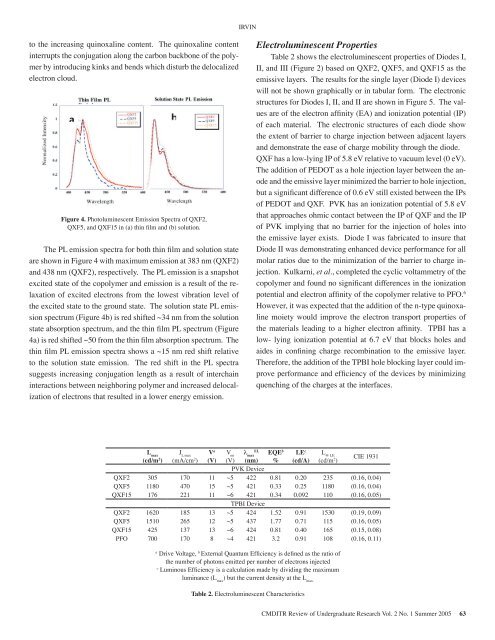
max bthinfilm(nm)438437428ion or inution orured insolutionsinglelm stater chainsthe thinties <strong>of</strong> atheirtion <strong>of</strong>It is understood that increased conjugation lengthleads to red shifted absorption. Therefore, thehigher energy absorption band <strong>of</strong> the QXF15relative to QXF2 is indicative <strong>of</strong> decreasingconjugation length due to the increasingto the increasingquinoxalinequinoxalinecontent.content.The quinoxalineThe quinoxalinecontentcontentinterrupts interrupts the conjugation the conjugation along the carbon along backbone the carbon <strong>of</strong> the polymerby introducing backbone <strong>of</strong> kinks the and polymer bends which by introducing disturb the kinks delocalizedelectron and cloud. bends which disturb the delocalized electroncloud.Normalized Intensity1.210.80.60.40.20aThin Film PLE i i400 450 500 550 600Wavelength( )QXF2QXF5QXF15Solution State PL EmissionQXF2QXF5QXF15450 500 550 600Wavelength( )Figure 4. Photoluminescent Emission Emission Spectra <strong>of</strong> Spectra QXF2, <strong>of</strong>in film QXF2, QXF5, QXF5, and QXF15 and QXF15 in (a) thin in film (a) and thin (b) film solution. and (b)and 3b. solution.tion <strong>of</strong>The PL The emission PL emission spectra for spectra both thin for both film and thin solution film statevarious and solution state are shown in Figure 4 withare shown in Figure 4 with maximum emission at 383 nm (QXF2)ate and maximum emission at 383 nm (QXF2) and 438<strong>of</strong> the and 438nmnm (QXF2),(QXF2),respectively.respectively.TheThePLPLemissionemissionisisa snapshotasorption excited state snapshot <strong>of</strong> the excited copolymer state and <strong>of</strong> emission the copolymer is a result and <strong>of</strong> the relaxationemission <strong>of</strong> excited is electrons a result <strong>of</strong> from the the relaxation lowest vibration <strong>of</strong> excited level <strong>of</strong>QXF2the excited electrons state to from the ground the lowest state. vibration The solution level state <strong>of</strong> theQXF5PL emissionspectrum excited (Figure state to 4b) the is red ground shifted state. ~34 nm The from solution the solutionQXF15state PL emission spectrum (Figure 4b) is redstate absorption spectrum, and the thin film PL spectrum (Figureshifted ~34 nm from the solution state4a) is redabsorptionshifted ~50spectrum,from the thinandfilmtheabsorptionthin filmspectrum.PLThethin film spectrum PL emission (Figure spectra 4a) is shows red shifted a ~15 nm ~50 red from shift the relativeto the solution thin film state absorption emission. spectrum. The red The shift thin film the PL spectrasuggests emission increasing spectra conjugation shows length a ~15 as a nm result red <strong>of</strong> shift450 500interchaininteractions relative between to the neighboring solution state polymer emission. and increased The red delocalization<strong>of</strong> electrons that resulted in a lower energyshift in the PL spectra suggests increasingQXF5,emission.bIRVINElectroluminescent PropertiesTable 2 shows the electroluminescent properties <strong>of</strong> Diodes I,II, and III (Figure 2) based on QXF2, QXF5, and QXF15 as theemissive layers. The results for the single layer (Diode I) deviceswill not be shown graphically or in tabular form. The electronicstructures for Diodes I, II, and II are shown in Figure 5. The valuesare <strong>of</strong> the electron affinity (EA) and ionization potential (IP)<strong>of</strong> each material. The electronic structures <strong>of</strong> each diode showthe extent <strong>of</strong> barrier to charge injection between adjacent layersand demonstrate the ease <strong>of</strong> charge mobility through the diode.QXF has a low-lying IP <strong>of</strong> 5.8 eV relative to vacuum level (0 eV).The addition <strong>of</strong> PEDOT as a hole injection layer between the anodeand the emissive layer minimized the barrier to hole injection,but a significant difference <strong>of</strong> 0.6 eV still existed between the IPs<strong>of</strong> PEDOT and QXF. PVK has an ionization potential <strong>of</strong> 5.8 eVthat approaches ohmic contact between the IP <strong>of</strong> QXF and the IP<strong>of</strong> PVK implying that no barrier for the injection <strong>of</strong> holes intothe emissive layer exists. Diode I was fabricated to insure thatDiode II was demonstrating enhanced device performance for allmolar ratios due to the minimization <strong>of</strong> the barrier to charge injection.Kulkarni, et al., completed the cyclic voltammetry <strong>of</strong> thecopolymer and found no significant differences in the ionizationpotential and electron affinity <strong>of</strong> the copolymer relative to PFO. 6However, it was expected that the addition <strong>of</strong> the n-type quinoxalinemoiety would improve the electron transport properties <strong>of</strong>the materials leading to a higher electron affinity. TPBI has alow- lying ionization potential at 6.7 eV that blocks holes andaides in confining charge recombination to the emissive layer.Therefore, the addition <strong>of</strong> the TPBI hole blocking layer could improveperformance and efficiency <strong>of</strong> the devices by minimizingquenching <strong>of</strong> the charges at the interfaces.L max(cd/m 2 )J L max(mA/cm 2 )V a(V)V onλ maxELEQE b%LE c(cd/A)L @ LE(cd/m 2 )CIE 1931(V) (nm)PVK DeviceQXF2 305 170 11 ~5 422 0.81 0.20 235 (0.16, 0.04)QXF5 1180 470 15 ~5 421 0.33 0.25 1180 (0.16, 0.04)QXF15 176 221 11 ~6 421 0.34 0.092 110 (0.16, 0.05)TPBI DeviceQXF2 1620 185 13 ~5 424 1.52 0.91 1530 (0.19, 0.09)QXF5 1510 265 12 ~5 437 1.77 0.71 115 (0.16, 0.05)QXF15 425 137 13 ~6 424 0.81 0.40 165 (0.15, 0.08)PFO 700 170 8 ~4 421 3.2 0.91 108 (0.16, 0.11)aDrive Voltage, b External Quantum Efficiency is defined as the ratio <strong>of</strong>the number <strong>of</strong> photons emitted per number <strong>of</strong> electrons injectedcLuminous Efficiency is a calculation made by dividing the maximumluminance (L max) but the current density at the L max.Table 2. Electroluminescent CharacteristicsCMDITR Review <strong>of</strong> Undergraduate Research Vol. 2 No. 1 Summer <strong>2005</strong> 63