Student Project Abstracts 2005 - Pluto - University of Washington
Student Project Abstracts 2005 - Pluto - University of Washington
Student Project Abstracts 2005 - Pluto - University of Washington
You also want an ePaper? Increase the reach of your titles
YUMPU automatically turns print PDFs into web optimized ePapers that Google loves.
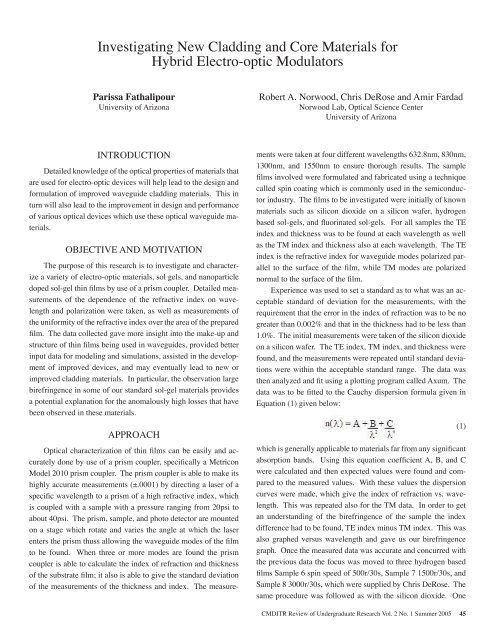
Investigating New Cladding and Core Materials forHybrid Electro-optic ModulatorsParissa Fathalipour<strong>University</strong> <strong>of</strong> ArizonaRobert A. Norwood, Chris DeRose and Amir FardadNorwood Lab, Optical Science Center<strong>University</strong> <strong>of</strong> ArizonaINTRODUCTIONDetailed knowledge <strong>of</strong> the optical properties <strong>of</strong> materials thatare used for electro-optic devices will help lead to the design andformulation <strong>of</strong> improved waveguide cladding materials. This inturn will also lead to the improvement in design and performance<strong>of</strong> various optical devices which use these optical waveguide materials.OBJECTIVE AND MOTIVATIONThe purpose <strong>of</strong> this research is to investigate and characterizea variety <strong>of</strong> electro-optic materials, sol gels, and nanoparticledoped sol-gel thin films by use <strong>of</strong> a prism coupler. Detailed measurements<strong>of</strong> the dependence <strong>of</strong> the refractive index on wavelengthand polarization were taken, as well as measurements <strong>of</strong>the uniformity <strong>of</strong> the refractive index over the area <strong>of</strong> the preparedfilm. The data collected gave more insight into the make-up andstructure <strong>of</strong> thin films being used in waveguides, provided betterinput data for modeling and simulations, assisted in the development<strong>of</strong> improved devices, and may eventually lead to new orimproved cladding materials. In particular, the observation largebirefringence in some <strong>of</strong> our standard sol-gel materials providesa potential explanation for the anomalously high losses that havebeen observed in these materials.APPROACHOptical characterization <strong>of</strong> thin films can be easily and accuratelydone by use <strong>of</strong> a prism coupler, specifically a MetriconModel 2010 prism coupler. The prism coupler is able to make itshighly accurate measurements (±.0001) by directing a laser <strong>of</strong> aspecific wavelength to a prism <strong>of</strong> a high refractive index, whichis coupled with a sample with a pressure ranging from 20psi toabout 40psi. The prism, sample, and photo detector are mountedon a stage which rotate and varies the angle at which the laserenters the prism thuss allowing the waveguide modes <strong>of</strong> the filmto be found. When three or more modes are found the prismcoupler is able to calculate the index <strong>of</strong> refraction and thickness<strong>of</strong> the substrate film; it also is able to give the standard deviation<strong>of</strong> the measurements <strong>of</strong> the thickness and index. The measurementswere taken at four different wavelengths 632.8nm, 830nm,1300nm, and 1550nm to ensure thorough results. The samplefilms involved were formulated and fabricated using a techniquecalled spin coating which is commonly used in the semiconductorindustry. The films to be investigated were initially <strong>of</strong> knownmaterials such as silicon dioxide on a silicon wafer, hydrogenbased sol-gels, and fluorinated sol-gels. For all samples the TEindex and thickness was to be found at each wavelength as wellas the TM index and thickness also at each wavelength. The TEindex is the refractive index for waveguide modes polarized parallelto the surface <strong>of</strong> the film, while TM modes are polarizednormal to the surface <strong>of</strong> the film.Experience was used to set a standard as to what was an acceptablestandard <strong>of</strong> deviation for the measurements, with therequirement that the error in the index <strong>of</strong> refraction was to be nogreater than 0.002% and that in the thickness had to be less than1.0%. The initial measurements were taken <strong>of</strong> the silicon dioxideon a silicon wafer. The TE index, TM index, and thickness werefound, and the measurements were repeated until standard deviationswere within the acceptable standard range. The data wasthen analyzed and fit using a plotting program called Axum. Thedata was to be fitted to the Cauchy dispersion formula given inEquation (1) given below:which is generally applicable to materials far from any significantabsorption bands. Using this equation coefficient A, B, and Cwere calculated and then expected values were found and comparedto the measured values. With these values the dispersioncurves were made, which give the index <strong>of</strong> refraction vs. wavelength.This was repeated also for the TM data. In order to getan understanding <strong>of</strong> the birefringence <strong>of</strong> the sample the indexdifference had to be found, TE index minus TM index. This wasalso graphed versus wavelength and gave us our birefringencegraph. Once the measured data was accurate and concurred withthe previous data the focus was moved to three hydrogen basedfilms Sample 6 spin speed <strong>of</strong> 500r/30s, Sample 7 1500r/30s, andSample 8 3000r/30s, which were supplied by Chris DeRose. Thesame procedure was followed as with the silicon dioxide. One(1)CMDITR Review <strong>of</strong> Undergraduate Research Vol. 2 No. 1 Summer <strong>2005</strong> 45


