Student Project Abstracts 2005 - Pluto - University of Washington
Student Project Abstracts 2005 - Pluto - University of Washington
Student Project Abstracts 2005 - Pluto - University of Washington

Create successful ePaper yourself
Turn your PDF publications into a flip-book with our unique Google optimized e-Paper software.
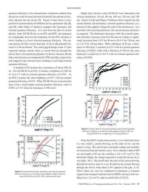
MONTGOMERYquantum efficiency is the measurement <strong>of</strong> photons emitted fromthe device in the forward direction divided by the amount <strong>of</strong> electronsinjected into the device [5]. Figure 4 (top) shows a comparison<strong>of</strong> current density for different device geometries (1), (2),and (3), while Figure 4 (bottom) compares the luminance andexternal quantum efficiency. It is seen from the plot <strong>of</strong> currentdensity, when XZ-III-20 acts as an ETL and HTL, the responsesare comparable, however the luminance for the ETL structure islower, leading to a lower external quantum efficiency. The currentdensity for (3) is lower than that <strong>of</strong> (1) or (2) primarily becauseit is 40 nm thicker. The small jagged bumps in the J-V plotrepresent leakage current; there is current flowing through thedevice that is not producing photons. In device structure (3) theholes and electrons are transported by TPD and AlQ 3respectivelyand trapped in the emission layer resulting in such high externalquantum efficiency.A standard LCD monitor has a luminance <strong>of</strong> about 300 cd/m 2 . For XZ-III-20 as an ETL, it reaches a brightness <strong>of</strong> 300 cd/m 2 at 6.3 V with an external quantum efficiency <strong>of</strong> 0.55%. Asan HTL it reaches the same brightness at 5.8 V with an externalquantum efficiency <strong>of</strong> 0.6%. When XZ-III-20 acts as an emissionlayer it has a much higher external quantum efficiency value <strong>of</strong>0.95% at 7.6 V when the luminance is 300 cd/m 2 .Single layer devices using XZ-III-20 were fabricated withvarying thicknesses: 50 nm, 80 nm, 100 nm, 120 nm, and 150nm. Figure 5 (top) and Figure 5 (bottom) show respectively thecurrent density and luminance, external quantum efficiency as afunction <strong>of</strong> the applied voltage for each <strong>of</strong> the thicknesses. It isseen that with increasing thickness, the current density decreasesas expected. The luminance decreases while the external quantumefficiency increases, however the turn-on voltage is significantlyincreased from 3.6 V for 50 nm to 10.4 V for 150 nm, andto 11.6 V for 120 nm thick. With a thickness <strong>of</strong> 50 nm, a luminance<strong>of</strong> 300 cd/m 2 is reached at 6.5 V with an external quantumefficiency <strong>of</strong> 0.08%; while with a thickness <strong>of</strong> 150 nm, the sameluminance is achieved at 16.9 V with an external quantum efficiency<strong>of</strong> 0.09%.Figure 5. Current density (top) and luminance and external quantumefficiency (bottom) as a function <strong>of</strong> the applied voltage <strong>of</strong> devicesusing XZ-III-20 as a single layer <strong>of</strong> varying thickness.Figure 4. Current density (top), luminance and external quantumefficiency (bottom) as a function <strong>of</strong> the applied voltage <strong>of</strong> devicesusing XZ-III-20 as an ETL, HTL, and emission layer.From the OFET output characteristic, it is evident that thereis a very small I Dcurrent flowing, on the order <strong>of</strong> nA, and thesignal is noisy. The on/<strong>of</strong>f ratio, threshold voltage and mobilityare extracted from the transfer curve. For a channel width <strong>of</strong> 500nm and length <strong>of</strong> 50 nm, the mobility is 4.0 x 10 -6 cm 2 /Vs, Thethreshold voltage, the voltage required to switch the device on, isvery high, -56 V. The on/<strong>of</strong>f ratio, the ratio <strong>of</strong> the current flowingthrough the device when it is on, divided by the current flowingthrough the device when there is 0V applied at the gate, is 10.These values are very low compared to pentacene, a commonorganic hole-transport material used in OFETs, having a hole mobility<strong>of</strong> μ = 2.4 cm 2 /V-s and an on/<strong>of</strong>f ratio <strong>of</strong> 10 8 [3].CMDITR Review <strong>of</strong> Undergraduate Research Vol. 2 No. 1 Summer <strong>2005</strong> 87