SYNTHESIS AND CHARACTERIZATION OF EXTENDED SQUARAINE COMPOUNDSScheme 4. Synthesis <strong>of</strong> the desired product, squaraine (11) using (3).Dibutyl-{4-[2-(3,4-dibutoxy-thiophen-2-yl)-vinyl]-phenyl}-amine, (7) was then treated with butyl lithium in dry THF at 0 ºC,after two hours DMF was added and left overnight all under N 2.The red solution was washed with water and extracted with ethylacetate (3×). The organic phase is collected and dried over magnesiumsulfate. The concentrated solution was purified by columnchromatography, eluent 10:1 hexanes to ethyl acetate in silica togive (8). 3,4-dibutoxy-5-[2-(4-dibutylamino-phenyl)-vinyl]-thiophene-2-carbaldehyde,(8), was reduced by sodium borohydridein ethanol, similar to the procedure for compound (5), which wasthen reacted with tri-ethyl phosphate in iodine at 0 ºC and leftovernight under N 2. Vacuum distillation was performed on thesolution for two hours and purified by column chromatography,eluent 4:1 hexanes to ethyl acetate to yield (9).Compound (3), 1-(2-ethyl-hexyl)-1H-pyrrole-2-carbaldehydewas reacted with {3,4-Dibutoxy-5-[2-(4-dibutylamino-phenyl)-vinyl]-thiophen-2-ylmethyl}-phosphonicacid diethyl ester,compound (9), in dry THF and a solution <strong>of</strong> potassium tert-butoxidein dry THF by a Horner-Emmons Condensation, underN 2,for an hour and a half. The concentrated oil was purified bycolumn chromatography, eluent 10:1 hexanes to ethyl acetate insilica to give rise to compound (10). Dibutyl-{4-[2-(3,4-dibu-toxy-5-{2-[1-(2-ethyl-hexyl)-1H-pyrrol-2-yl]-vinyl}-thiophen-2-yl)-vinyl]-phenyl}-amine, (10) is treated with squaric acid togive the desired compound (11) Squaraine.CONCLUSIONAfter several failed reactions, it was determined that an alkylatedpyrrole carbaldehyde can be synthesized in high yield.Many <strong>of</strong> these reactions caused side products which requiredcareful purification techniques that took longer than expected.Therefore, the desired product squaraine is one reaction awayfrom completion. After pure squaraine is obtained, tests will beperformed on the organic dye to determine its efficacy in producingoptical quality, thin films.REFERENCESM.J. Plater, T. Jackson. Tetrahedron 59 (2003). pages 4673-4685(page 4679).ACKNOWLEDGEMENTSResearch support is gratefully acknowledged from the NationalScience Foundation Center on Materials and Devices forInformation Technology Research (CMDITR), DMR-0120967.Tehetena Mesganaw is currently attending the Georgia Institute <strong>of</strong>Technology and majoring in Chemistry. After graduation im Fall 2006,she plans to attend graduate school and obtain her Ph.D in OrganicChemistry. From there, she plans to do research on the AIDS epidemic.82 CMDITR Review <strong>of</strong> Undergraduate Research Vol. 2 No. 1 Summer <strong>2005</strong>
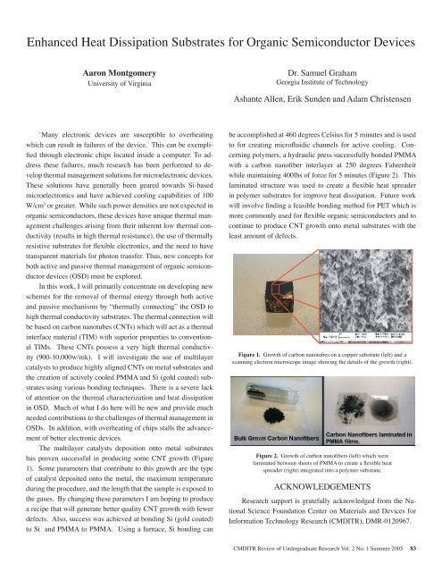
Enhanced Heat Dissipation Substrates for Organic Semiconductor DevicesAaron Montgomery<strong>University</strong> <strong>of</strong> VirginiaDr. Samuel GrahamGeorgia Institute <strong>of</strong> TechnologyAshante Allen, Erik Sunden and Adam Christensen`Many electronic devices are susceptible to overheatingwhich can result in failures <strong>of</strong> the device. This can be exemplifiedthrough electronic chips located inside a computer. To addressthese failures, much research has been performed to developthermal management solutions for microelectronic devices.These solutions have generally been geared towards Si-basedmicroelectronics and have achieved cooling capabilities <strong>of</strong> 100W/cm 2 or greater. While such power densities are not expected inorganic semiconductors, these devices have unique thermal managementchallenges arising from their inherent low thermal conductivity(results in high thermal resistance), the use <strong>of</strong> thermallyresistive substrates for flexible electronics, and the need to havetransparent materials for photon transfer. Thus, new concepts forboth active and passive thermal management <strong>of</strong> organic semiconductordevices (OSD) must be explored.In this work, I will primarily concentrate on developing newschemes for the removal <strong>of</strong> thermal energy through both activeand passive mechanisms by “thermally connecting” the OSD tohigh thermal conductivity substrates. The thermal connection willbe based on carbon nanotubes (CNTs) which will act as a thermalinterface material (TIM) with superior properties to conventionalTIMs. These CNTs possess a very high thermal conductivity(900-10,000w/mk). I will investigate the use <strong>of</strong> multilayercatalysts to produce highly aligned CNTs on metal substrates andthe creation <strong>of</strong> actively cooled PMMA and Si (gold coated) substratesusing various bonding techniques. There is a severe lack<strong>of</strong> attention on the thermal characterization and heat dissipationin OSD. Much <strong>of</strong> what I do here will be new and provide muchneeded contributions to the challenges <strong>of</strong> thermal management inOSDs. In addition, with overheating <strong>of</strong> chips stalls the advancement<strong>of</strong> better electronic devices.The multilayer catalysts deposition onto metal substrateshas proven successful in producing some CNT growth (Figure1). Some parameters that contribute to this growth are the type<strong>of</strong> catalyst deposited onto the metal, the maximum temperatureduring the procedure, and the length that the sample is exposed tothe gases. By changing these parameters I am hoping to producea recipe that will generate better quality CNT growth with fewerdefects. Also, success was achieved at bonding Si (gold coated)to Si and PMMA to PMMA. Using a furnace, Si bonding canbe accomplished at 460 degrees Celsius for 5 minutes and is usedto for creating micr<strong>of</strong>luidic channels for active cooling. Concerningpolymers, a hydraulic press successfully bonded PMMAwith a carbon nan<strong>of</strong>iber interlayer at 250 degrees Fahrenheitwhile maintaining 400lbs <strong>of</strong> force for 5 minutes (Figure 2). Thislaminated structure was used to create a flexible heat spreaderin polymer substrates for improve heat dissipation. Future workwill involve finding a feasible bonding method for PET which ismore commonly used for flexible organic semiconductors and tocontinue to produce CNT growth onto metal substrates with theleast amount <strong>of</strong> defects.Figure 1. Growth <strong>of</strong> carbon nanotubes on a copper substrate (left) and ascanning electron microscope image showing the details <strong>of</strong> the growth (right).Figure 2. Growth <strong>of</strong> carbon nan<strong>of</strong>ibers (left) which werelaminated between sheets <strong>of</strong> PMMA to create a flexible heatspreader (right) integrated into a polymer substrate.ACKNOWLEDGEMENTSResearch support is gratefully acknowledged from the NationalScience Foundation Center on Materials and Devices forInformation Technology Research (CMDITR), DMR-0120967.CMDITR Review <strong>of</strong> Undergraduate Research Vol. 2 No. 1 Summer <strong>2005</strong> 83
- Page 2 and 3:
The material is based upon work sup
- Page 4 and 5:
TABLE OF CONTENTSSynthesis of Dendr
- Page 6 and 7:
6 CMDITR Review of Undergraduate Re
- Page 8 and 9:
SYNTHESIS OF DENDRIMER BUILDING BLO
- Page 10 and 11:
throughout the work period. Five su
- Page 12 and 13:
12 CMDITR Review of Undergraduate R
- Page 14 and 15:
BARIUM TITANATE DOPED SOL-GEL FOR E
- Page 16 and 17:
BARIUM TITANATE DOPED SOL-GEL FOR E
- Page 18 and 19:
SYNTHESIS OF NORBORNENE MONOMER OF
- Page 20:
20 CMDITR Review of Undergraduate R
- Page 23 and 24:
using different reaction conditions
- Page 25 and 26:
Synthesis of Nonlinear Optical-Acti
- Page 27 and 28:
quality of the XRD structures wasca
- Page 29 and 30:
Behavioral Properties of Colloidal
- Page 32 and 33: Transmission electron microscopy ha
- Page 34 and 35: 34 CMDITR Review of Undergraduate R
- Page 36 and 37: areorient themselves with the elect
- Page 38 and 39: Fabry-Perot modulators with electro
- Page 40 and 41: 40 CMDITR Review of Undergraduate R
- Page 42 and 43: QUANTIZED HAMILTON DYNAMICS APPLIED
- Page 44 and 45: 44 CMDITR Review of Undergraduate R
- Page 46 and 47: INVESTIGATING NEW CLADDING AND CORE
- Page 48 and 49: Dr. Robert NorwoodChris DeRoseAmir
- Page 50 and 51: SYNTHESIS OF TPD-BASED COMPOUNDS FO
- Page 52 and 53: SYNTHESIS OF TPD-BASED COMPOUNDS FO
- Page 54 and 55: OPTIMIZING HYBRID WAVEGUIDESpropaga
- Page 56 and 57: At closer spaces the second undesir
- Page 58 and 59: SYNTHESIS AND ANALYSIS OF THIOL-STA
- Page 60 and 61: 60 CMDITR Review of Undergraduate R
- Page 62 and 63: QUINOXALINE-CONTAINING POLYFLUORENE
- Page 64 and 65: QUINOXALINE-CONTAINING POLYFLUORENE
- Page 66 and 67: 66 CMDITR Review of Undergraduate R
- Page 68 and 69: SYNTHESIS OF DENDRON-FUNCTIONALIZED
- Page 70 and 71: 70 CMDITR Review of Undergraduate R
- Page 72 and 73: BUILDING AN OPTICAL OXIMETER TO MEA
- Page 74 and 75: 74 CMDITR Review of Undergraduate R
- Page 76 and 77: 76 CMDITR Review of Undergraduate R
- Page 78 and 79: TOWARD MOLECULAR RESOLUTION C-AFM W
- Page 80 and 81: TOWARD MOLECULAR RESOLUTION C-AFM W
- Page 84 and 85: My name is Aaron Montgomery and I a
- Page 86 and 87: 1,1-DIPHENYL-2,3,4,5-TETRAKIS(9,9-D
- Page 88 and 89: 1,1-DIPHENYL-2,3,4,5-TETRAKIS(9,9-D
- Page 90 and 91: EFFECTS OF SURFACE CHEMISTRY ON CAD
- Page 92 and 93: EFFECTS OF SURFACE CHEMISTRY ON CAD
- Page 94 and 95: 94 CMDITR Review of Undergraduate R
- Page 96 and 97: SYNTHESIS OF A POLYENE EO CHROMOPHO
- Page 98 and 99: SYNTHESIS OF A POLYENE EO CHROMOPHO
- Page 102 and 103: 102 CMDITR Review of Undergraduate
- Page 104 and 105: CHARACTERIZATION OF THE MOLECULAR P
- Page 106 and 107: 106 CMDITR Review of Undergraduate
- Page 108 and 109: OPTIMIZATION OF SEMICONDUCTOR NANOP
- Page 110 and 111: OPTIMIZATION OF SEMICONDUCTOR NANOP
- Page 112 and 113: CHARACTERIZATION OF THE PHOTODECOMP
- Page 114 and 115: 114 CMDITR Review of Undergraduate
- Page 116 and 117: ELECTROLUMINESCENT PROPERTIES OF OR
- Page 118 and 119: 118 CMDITR Review of Undergraduate
- Page 120 and 121: DETERMINATION OF MOLECULAR ORIENTAT
- Page 122 and 123: DETERMINATION OF MOLECULAR ORIENTAT
- Page 124 and 125: HYDROGEL MATERIALS FOR TWO-PHOTON M
- Page 126 and 127: HYDROGEL MATERIALS FOR TWO-PHOTON M
- Page 128 and 129: THE DESIGN OF A FLUID DELIVERY SYST
- Page 130: THE DESIGN OF A FLUID DELIVERY SYST