CONFINAMIENTO NANOSC´OPICO EN ESTRUCTURAS ... - It works!
CONFINAMIENTO NANOSC´OPICO EN ESTRUCTURAS ... - It works!
CONFINAMIENTO NANOSC´OPICO EN ESTRUCTURAS ... - It works!
Create successful ePaper yourself
Turn your PDF publications into a flip-book with our unique Google optimized e-Paper software.
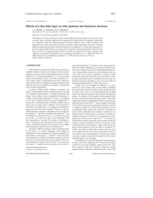
Confinamientos espacial y másico 163JOURNAL OF APPLIED PHYSICS VOLUME 94, NUMBER 7 1 OCTOBER 2003Effects of a thin AlAs layer on InAs quantum dot electronic structureJ. L. Movilla, J. I. Climente, and J. Planelles a)Departament de Ciències Experimentals, UJI, Box 224, E-12080 Castelló, SpainReceived 16 June 2003; accepted 15 July 2003The influence of a thin AlAs layer 1 nm located at different positions inside a GaAs matrix on theelectronic states of nearby deposited InAs quantum dots is theoretically investigated. Calculationsare performed within the three-dimensional one-band effective mass model including massdependence on energy and position. In order to provide a realistic description of the wave functiondiffusion outside the dot, finite confinement barriers are considered. <strong>It</strong> is shown that the presence ofthe AlAs high potential barrier can account for the reported experimental blueshift when the AlAslayer is grown as a capping material, but this is not the case when the AlAs layer is grown in thesubstrate. An alternative explanation of the experimental data Kim et al., J. Appl. Phys. 91, 50552002 based on our calculations is proposed. © 2003 American Institute of Physics.DOI: 10.1063/1.1606519I. INTRODUCTIONSelf-assembled quantum dots QDs have attracted considerableattention in recent years because of their excellentproperties as active media in semiconductor devices such asQD lasers 1,2 or infrared photodetectors. 3–5 The most widelystudied self-assembled system, InAs QDs embedded in aGaAs matrix, shows a photoluminescence PL peak typicallyaround 1050 nm. 6 Shifting this spectral channel towarddifferent emission or absorption wavelengths is essential formore extensive applications.In order to obtain shorter emission wavelengths, thechoice of high potential barrier materials has been revealedas a valuable control parameter. 12 <strong>It</strong> enables shifting the QDenergy levels without severe composition fluctuations, incontrast to QD alloying techniques. 7,8 Al x Ga 1x As matricesare the most common choice for practical applications 9,10because the corresponding lattice constants, similar to that ofGaAs, lead to similar strain conditions for the growth ofInAs QDs. 11 By using Al x Ga 1x As matrices, PL blueshifts aslarge as 612 meV have been reported. 12 Moreover, other desirablebenefits for practical applications, such as high thermalstability 12,13 and high controllable QDs densities 14,15 canbe obtained by using InAs/Al x Ga 1x As systems. However,the Al x Ga 1x As matrix also shows some drawbacks. Themost important are a weaker PL emission as compared tothat of InAs/GaAs QDs because of the presence of lowdensitynonradiative channels in the barrier 16 and a higherpeak broadening caused by dot size fluctuations. 12Recently, a different technique which incorporates mostof the Al x Ga 1x As matrix advantages while eluding itsdrawbacks has been introduced: The QDs are embedded in aGaAs matrix, in which one 17–19 or more 20,21 thin AlAs layersare deposited near the QD. By tuning the position of the thinAlAs layer, several benefits have been reported. These include,blueshifts as large as 500 meV Ref. 21, an increaseddot density, 18 a higher dot size uniformity derived from aa Electronic mail: planelle@exp.uji.esreduced In segregation, 19 and others. Due to these properties,thin AlAs barriers engineering is an attractive field for practicaldevice design. In the case of infrared photodetector devices,reduced dark currents have been obtained with thinAlAs layers even at room temperature, 22 leading to largerdetectivities than those observed in the InAs/GaAs system.In spite of the great interest of utilizing thin AlAs layers, notheoretical study has attempted so far to assess the effect ofthin high potential barriers on QDs energy levels.In this work, we investigate the influence of a 1-nmthickAlAs layer, located inside a GaAs matrix at differentbut close distances from InAs QDs, on their conduction-bandlow-lying states. We use the three-dimensional one-bandmodel with position-dependent band extrema and effectivemasses. The validity of such model for self-assembled QDshas been widely tested with fairly good results. 23 Our modeladditionally includes nonparabolicity effects, as these play animportant role for InAs QDs. 24,25 Since a realistic descriptionof the electron wave function spread into the barrier materialis required to predict the overlap with the AlAs layer, we usean appropiate finite square-well potential. 26 The effect ofstrain on the conduction band is mainly to modify the confiningpotential, which becomes a function of position, althoughan average over the QD, as we assume in our calculations,has been proven to work well. 23,27 The strain alsomodifies the curvature of the bulk band causing the effectivemasses to become anisotropic. However, in the case of theconduction band, this anisotropy is rather small and an isotropicelectron effective mass can safely be employed. 23,28Finally, the change in bulk band curvatures may also causesome variation of the actual value of the effective mass. Inour position and energy-dependent effective-mass model,such mass variation is implicitly accounted for by the straininducedchanges in the band gap.Our results are in reasonable agreement with experimentaldata of thin AlAs capping layers. 19 However, they cannotaccount for the large blueshifts observed when the AlAslayer is grown in the GaAs substrate. 17 This fact stronglysuggests that the explanation of these blueshifts as due to the0021-8979/2003/94(7)/4515/5/$20.00 4515© 2003 American Institute of Physics


