CONFINAMIENTO NANOSC´OPICO EN ESTRUCTURAS ... - It works!
CONFINAMIENTO NANOSC´OPICO EN ESTRUCTURAS ... - It works!
CONFINAMIENTO NANOSC´OPICO EN ESTRUCTURAS ... - It works!

Create successful ePaper yourself
Turn your PDF publications into a flip-book with our unique Google optimized e-Paper software.
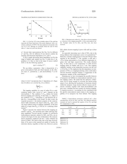
Confinamiento dieléctrico 223TRAPPING ELECTRONS IN SEMICONDUCTOR AIR¼PHYSICAL REVIEW B 73, 235350 2006FIG. 3. V 0 see Eq. 2 vs the air bubble radius R. The solid linerepresents the linear regression of the points displayed, with a correlationcoefficient of 0.9974. The data employed corresponds to thecase of m * =0.5, although we essentially obtain the same fit whenother m * values are used not shown.m * . Several other representations like Fig. 2a for differentm * and Fig. 2b for different R not shown confirm themeaning and functional dependence of V 0 and A.V 0 has a simple decreasing linear dependence on R in therange of bubble radii studied see Fig. 3 while the m * dependenceof A that we find in the range of masses studied0.03–1 fits the following equation:Am * = 0.83m * 0.13 .We can define a parameter t that is characteristic of agiven semiconductor bulk and which depends on the effectivemass m * , permittivity , and electroaffinitiy V as follows:3t = LnA , 4Vwhere A=Am * incorporates the m * dependence of t. Equation4 allows us to rewrite Eq. 2 as follows:V maxV 01V = t.The trapping capability of a pore of radius R in a semiconductormatrix with a given m * and depends on theelectroaffinity V. The condition V=V max defines the borderbetween trapping and scattering. At this limit, i.e., subject tothe condition V=V max , t determines V 0 and therefore the radiusR max corresponding to this border. In other words, thetrapping parameter t an intrinsic property of the semiconductorbulk determines the largest radius R max that a porecan reach without losing its trapping capabilities. If the poreradius R is larger than R max it will act as a scattering centerinstead. 35Figure 4 presents the relation between this trapping parametert and R max , the maximum pore radius allowing trappingcapabilities. Several specific examples of well-knownsemiconductor materials, namely Si, SiO 2 , and TiO 2 , are enclosedin the figure for the sake of illustration. The semiconductorparameters employed and the t values obtained areshown in Table I. We observe that, due to the large electroaffinityof Si, pores in this material are unable to localize theelectronic density, regardless of their size. However, porous5FIG. 4. Maximum pore radius R max that allows electron trappingas a function of the trapping parameter t of the semiconductor matrix.Example values for Si, SiO 2 , and TiO 2 have also beenenclosed.SiO 2 admits electron trapping in pores with radii up to about13 nm.An especially interesting case is that of TiO 2 , due to thestrong influence that temperature exerts on its permittivity. 25Dielectric constants ranging from 6 to beyond 150 have beenreported in the literature. 25,26 We consider =100 and =30 as being representative of two different temperature regimeslow and high, respectively. The results obtainedFig. 4 show that at a low temperature =100 electrontrapping holds for bubble radii up to 7 nm. This trappingcapability vanishes as the temperature increases see the case=30 in Fig. 4. We emphasize that this dependence on temperatureof TiO 2 as a trapping/scattering center could inducerelevant electronic transport changes vs temperature in thenanoporous samples of this semiconductor. 36Summing up, we have investigated the possible behaviorof nanopores air bubbles in semiconductor materials as carriertrapping centers. We found that the dielectric confinementcan be strong enough to overcome the barrier-actingnature of air, allowing the localization of electronic densitywithin the nanopore. Large electron effective masses and dielectricconstants, together with small electroaffinities andpore sizes, constitute the best scenario for electron trapping.A trapping parameter t accounting for the contribution thatthe specific semiconductor matrix makes to the trapping capabilityof its nanopores has been defined. This trappingTABLE I. Semiconductor parameters employed and t valuescalculated Eq. 4 for Si, SiO 2 , and TiO 2 . Two different dielectricconstants are used to represent the regimes of low T↓ and highT↑ temperatures in TiO 2 .V eV m * t eV −1 Si 4.0 a 0.26 b 12 a 0.53SiO 2 0.9 a 0.5 c 4 b 1.22TiO 2 3.9 a 1.0 d 100 T↓ 1.1330 T↑ 0.82a Reference 27.b Reference 22.c Reference 28.d Reference 29.235350-3