CSEM Scientific and Technical Report 2008
CSEM Scientific and Technical Report 2008
CSEM Scientific and Technical Report 2008

Create successful ePaper yourself
Turn your PDF publications into a flip-book with our unique Google optimized e-Paper software.
SUMO – SUrface MOdified Vision Systems<br />
T. Baechler, C. Lotto, E. Franzi, P.-F. Ruedi, P. Heim, M. Morgan, A. Stuck, M. Schnieper, C. Winnewisser, R. Stanley, A. Dunbar,<br />
M. Chrapa, C. Bosshard, G. Spinola Durante, C. Urban, R. Kaufmann, A. Dommann<br />
Many different “light-modifying layer technologies” are available at <strong>CSEM</strong>. In this project, <strong>CSEM</strong> wants to investigate the most promising<br />
combinations to achieve stable color, polarization, <strong>and</strong> magnification effects using replication <strong>and</strong> plasmonic techniques on top of image sensors.<br />
Other aspects include the integration of OLED light sources at the surface of an image sensor, the use of thin <strong>and</strong> thick Germanium layers for<br />
effective NIR (near-IR) <strong>and</strong> X-ray direct detectors, <strong>and</strong> finally the integration of a DSP-core as close as possible to the active imaging part to locally<br />
process huge amounts of raw image data.<br />
The principal goal is to study heterogeneous systems based<br />
on smart combinations of CMOS image sensors <strong>and</strong> microelectrode<br />
arrays (MEAs) with additional layers placed on top<br />
of those detectors. These layers include the development <strong>and</strong><br />
characterization of polarization <strong>and</strong> colour (spectral) filters<br />
made of zero-order replication grids <strong>and</strong> plasmon structures.<br />
The development of direct detectors for X-ray imaging (without<br />
any additional scintillator plate) providing higher sensitivity <strong>and</strong><br />
spatial resolution is another important topic of the SUMO-MIP.<br />
Two basic approaches are pursued. The first one is based on<br />
the combination of a germanium (Ge) wafer with a dedicated<br />
read-out integrated circuit (ROIC) <strong>and</strong> bond bumping<br />
technologies. In this case one of the crucial aspects is the<br />
interconnection of the Ge wafer with the ROIC. <strong>CSEM</strong><br />
packaging experts are working on bump techniques for 2Darrays<br />
at a pitch of less than 50 µm. First daisy chain test<br />
arrays are produced <strong>and</strong> will be characterized early 2009. The<br />
second approach targets the monolithic integration of Ge<br />
photodiodes in a CMOS process including circuitry. Thin Ge<br />
layers (3 µm) were successfully demonstrated as suitable for<br />
near infrared imaging. Thicker layers are under development<br />
for X-ray imaging.<br />
Organic light-emitting devices (OLEDs) have been prepared<br />
for on-imager integration. Figure 1 shows a working prototype<br />
device, which can be placed on or near an image detector, e.g.<br />
as part of highly miniaturized optical encoders or 3D Time-Of-<br />
Flight (3D-TOF) cameras. For the moment, modulation<br />
frequencies of some 100 kHz are possible, but still too low in<br />
the case of 3D-TOF applications.<br />
Figure 1: First OLED light source to be implemented on an imager<br />
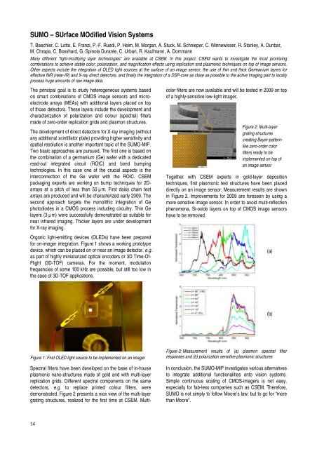
Spectral filters have been developed on the base of in-house<br />
plasmonic nano-structures made of gold <strong>and</strong> with multi-layer<br />
replication grids. Different spectral components on the same<br />
detectors, e.g. to replace printed colour filters, were<br />
demonstrated. Figure 2 presents a nice view of the multi-layer<br />
grating structures, realized for the first time at <strong>CSEM</strong>. Multi-<br />
14<br />
color filters are now available <strong>and</strong> will be tested in 2009 on top<br />
of a highly-sensitive low-light imager.<br />
Figure 2: Multi-layer<br />
grating structures<br />
creating Bayer-patternlike<br />
zero-order color<br />
filters ready to be<br />
implemented on top of<br />
an image sensor<br />
Together with <strong>CSEM</strong> experts in gold-layer deposition<br />
techniques, first plasmonic test structures have been placed<br />
directly on an image sensor. Measurement results are shown<br />
in Figure 3. Improvements for 2009 are foreseen by using a<br />
more sensitive image sensor. In order to avoid multi-reflection<br />
phenomena, Si-oxide layers on top of CMOS image sensors<br />
have to be removed.<br />
Figure 3: Measurement results of (a) plasmon spectral filter<br />
responses <strong>and</strong> (b) polarization sensitive plasmonic structures<br />
In conclusion, the SUMO-MIP investigates various alternatives<br />
to integrate additional functionalities onto vision systems.<br />
Simple continuous scaling of CMOS-imagers is not easy,<br />
especially for fab-less companies such as <strong>CSEM</strong>. Therefore,<br />
SUMO is not simply to follow Moore’s law, but to go for “more<br />
than Moore”.<br />
(a)<br />
(b)