CSEM Scientific and Technical Report 2008
CSEM Scientific and Technical Report 2008
CSEM Scientific and Technical Report 2008

You also want an ePaper? Increase the reach of your titles
YUMPU automatically turns print PDFs into web optimized ePapers that Google loves.
Design of RF Passives in 65 nm CMOS<br />
M. Kucera, F. Pengg, A. Vouilloz, J. Chabloz, R. Caseiro, N. Scolari, C. Monneron<br />
Continuous cost reductions have for years been among the prevailing driving factors in IC <strong>and</strong> RF Design. To meet the challenges of the latest<br />
process technologies, which have impressive gate densities of up to 800’000 gates per square millimeter, it is becoming increasingly important to<br />
reduce the size of passive devices. This article gives an insight how <strong>CSEM</strong> has leveraged its experience <strong>and</strong> know-how to meet customer<br />
requirements in a 65 nm CMOS technology.<br />
Gate density is among the key performance indicators in ultra<br />
deep-submicron CMOS technologies. Process technology<br />
advancements have provided the digital design community<br />
with impressive capabilities, almost doubling every 18 months<br />
the number of digital logic gates per square millimeter.<br />
Compared to digital design, constraints <strong>and</strong> requirements are<br />
very different for RF circuits: gate density is not a concern, but<br />
rather the size <strong>and</strong> quality of the RF blocks – generally<br />
determined by the RF passive devices – for a given<br />
performance. A major challenge in RF design is to optimise<br />
the design of integrated passive devices like inductors <strong>and</strong><br />
capacitors. For highly integrated RF transceivers requiring<br />
high performance or ultra low-power consumption, these<br />
integrated passive devices are of utmost importance as their<br />
achievable characteristics <strong>and</strong> quality factors will directly<br />
determine the radio performance. Realizing innovative CMOS<br />
radios [1] requires a thorough underst<strong>and</strong>ing of the achievable<br />
<strong>and</strong> limiting characteristics of integrated RF passive devices. It<br />
is thus essential to underst<strong>and</strong> the device physics, to be<br />
capable of measuring them using state-of-the art RF wafer<br />
probers up to frequencies of typically 50 GHz, to extract the<br />
device parameters <strong>and</strong> elaborate a simulation model that can<br />
be used by the RF IC designers.<br />
Silicon foundries generally propose a basic set of RF passive<br />
devices in their design kits (DK), which can be used in generic<br />
cases where current consumption, performance <strong>and</strong> size are<br />
not an issue. The reasons are that universally usable <strong>and</strong><br />
suitable RF inductors do not exist: every inductor has its own<br />
inductance value <strong>and</strong> self-resonance frequency due to its<br />
parasitics. Furthermore as the silicon foundry knows neither<br />
the operating frequency nor the required inductor value it can<br />
only propose a limited usability of the required device or at<br />
best some kind of scalable device. A further important<br />
limitation lies in the fact that the associated models are often<br />
only approximate, <strong>and</strong> rarely correct at the desired frequency<br />
or the available metal layers. This leads to inaccurate<br />
simulations <strong>and</strong> unpredictable results <strong>and</strong> specifications. This<br />
is furthermore aggravated by the fact that foundries frequently<br />
only support inductors integrated with the expensive RF<br />
options, something customers often want to avoid, <strong>and</strong> which<br />
is against the trend of using pure digital processes for<br />
complex SOCs.<br />
For these reasons <strong>CSEM</strong> has designed dedicated inductors<br />
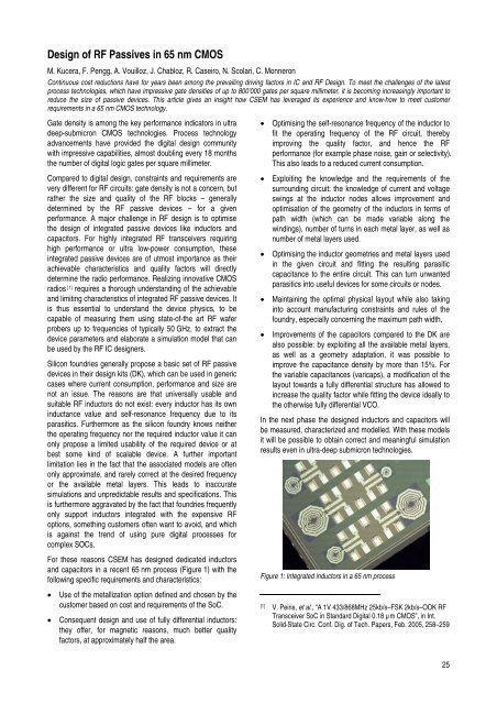
<strong>and</strong> capacitors in a recent 65 nm process (Figure 1) with the<br />
following specific requirements <strong>and</strong> characteristics:<br />
• Use of the metallization option defined <strong>and</strong> chosen by the<br />
customer based on cost <strong>and</strong> requirements of the SoC.<br />
• Consequent design <strong>and</strong> use of fully differential inductors:<br />
they offer, for magnetic reasons, much better quality<br />
factors, at approximately half the area.<br />
• Optimising the self-resonance frequency of the inductor to<br />
fit the operating frequency of the RF circuit, thereby<br />
improving the quality factor, <strong>and</strong> hence the RF<br />
performance (for example phase noise, gain or selectivity).<br />
This also leads to a reduced current consumption.<br />
• Exploiting the knowledge <strong>and</strong> the requirements of the<br />
surrounding circuit: the knowledge of current <strong>and</strong> voltage<br />
swings at the inductor nodes allows improvement <strong>and</strong><br />
optimisation of the geometry of the inductors in terms of<br />
path width (which can be made variable along the<br />
windings), number of turns in each metal layer, as well as<br />
number of metal layers used.<br />
• Optimising the inductor geometries <strong>and</strong> metal layers used<br />
in the given circuit <strong>and</strong> fitting the resulting parasitic<br />
capacitance to the entire circuit. This can turn unwanted<br />
parasitics into useful devices for some circuits or nodes.<br />
• Maintaining the optimal physical layout while also taking<br />
into account manufacturing constraints <strong>and</strong> rules of the<br />
foundry, especially concerning the maximum path width.<br />
• Improvements of the capacitors compared to the DK are<br />
also possible: by exploiting all the available metal layers,<br />
as well as a geometry adaptation, it was possible to<br />
improve the capacitance density by more than 15%. For<br />
the variable capacitances (varicaps), a modification of the<br />
layout towards a fully differential structure has allowed to<br />
increase the quality factor while fitting the device ideally to<br />
the otherwise fully differential VCO.<br />
In the next phase the designed inductors <strong>and</strong> capacitors will<br />
be measured, characterized <strong>and</strong> modelled. With these models<br />
it will be possible to obtain correct <strong>and</strong> meaningful simulation<br />
results even in ultra-deep submicron technologies.<br />
Figure 1: Integrated inductors in a 65 nm process<br />
[1] V. Peiris, et al., “A 1V 433/868MHz 25kb/s–FSK 2kb/s–OOK RF<br />
Transceiver SoC in St<strong>and</strong>ard Digital 0.18 µm CMOS”, in Int.<br />
Solid-State Circ. Conf. Dig. of Tech. Papers, Feb. 2005, 258–259<br />
25