CSEM Scientific and Technical Report 2008
CSEM Scientific and Technical Report 2008
CSEM Scientific and Technical Report 2008

Create successful ePaper yourself
Turn your PDF publications into a flip-book with our unique Google optimized e-Paper software.
Plasmon Based All Optical Switch<br />
R. Eckert, J. Dintinger • , T. Ebbesen • , R. P. Stanley<br />
Surface plasmons can strongly confine electric fields to metal-dielectric interfaces. Nano-structuring the metal can result in extraordinary optical<br />
transmission. J-aggregates are an efficient non-linear optical material. An optical switch with just a monolayer of J-aggregates on a nano-structured<br />
metal which can be pumped using a CW laser has been developed.<br />
Surface plasmons are electromagnetic surface waves which<br />
strongly confine the light at a metal dielectric interface. They<br />
play a key role in the extraordinary optical transmission (EOT)<br />
seen by Ebbesen in 1998. Ebbesen <strong>and</strong> co-workers showed<br />
that an array of subwavelength holes drilled in a metal film<br />
makes the otherwise opaque film transparent [1] . The concept<br />
of an ultrafast all–optical switch, which exploits EOT, has been<br />
recently demonstrated [2] .<br />
The all-optical switch consists of a metal film with a hole array<br />
covered with J-aggregates (Figure 1). J-aggregates (JA) are<br />
formed from cyanine molecules <strong>and</strong> have well-defined<br />
absorption b<strong>and</strong>s. The strong non-linearity of the J-aggregates<br />
means that when they are optically pumped the refractive<br />
index changes. This causes a shift in the peak transmission<br />
wavelength at which the EOT occurs. Therefore one beam of<br />
light (the probe beam) can be switched on <strong>and</strong> off by exciting<br />
the JA with a second beam of light (pump beam). The JA<br />
response time is 10 -12 seconds allowing very fast switching. As<br />
surface plasmons are tightly confined to the surface they are<br />
extremely sensitive to refractive index changes so switching<br />
could be achieved at very low powers.<br />
Figure 1: Concept of an all optical switch based on EOT<br />
In the work by Ditinger et al. JA were r<strong>and</strong>omly dispersed in a<br />
thick polymer film [2] . Here <strong>CSEM</strong> achieves the same effect but<br />
by using only a monolayer. The monolayer consists of a highly<br />
ordered JA formed by a process developed at <strong>CSEM</strong> using a<br />
template of self-assembled dendrimers. The remarkable<br />
absorption efficiency of these monolayers <strong>and</strong> the fact that the<br />
monolayer is very close to the metal allows optical switching<br />
at lower intensities.<br />
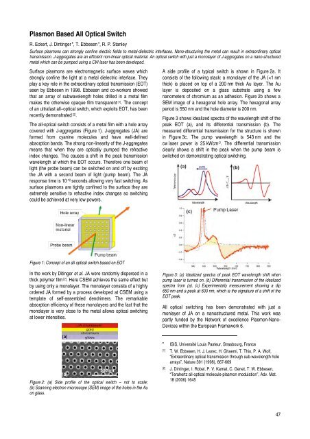
Figure 2: (a) Side profile of the optical switch – not to scale;<br />
(b) Scanning electron microscope (SEM) image of the holes in the Au<br />
on glass.<br />
A side profile of a typical switch is shown in Figure 2a. It<br />
consists of the following stack: a monolayer of the JA (