CSEM Scientific and Technical Report 2008
CSEM Scientific and Technical Report 2008
CSEM Scientific and Technical Report 2008

You also want an ePaper? Increase the reach of your titles
YUMPU automatically turns print PDFs into web optimized ePapers that Google loves.
Nanostructured Surfaces for High Sensitivity Biosensors in the Field of Safety <strong>and</strong><br />
Security<br />
B. Wenger, A.-M. Popa, E. Scolan, R. Pugin, G. Voirin<br />
Selective <strong>and</strong> sensitive monitoring of pesticides for food safety as well as the detection cocaine in the atmosphere of public buildings can both be<br />
achieved with optical biosensors featuring waveguide chips functionalized with specific antibodies. To further improve the sensitivity of these<br />
devices, nanostructuring techniques to increase the surface available for the biorecognition events were applied.<br />
The specificity of biosensors is probably their most<br />
outst<strong>and</strong>ing property. In fact, these devices take advantage of<br />
the extremely optimized recognition mechanisms offered by<br />
biological macromolecules to detect various targets with high<br />
selectivity. The task of the engineer is then to combine this<br />
molecular specificity with highly sensitive transducers in order<br />
to be able to detect the minimum number of recognition<br />
events.<br />
Over the past few years, <strong>CSEM</strong> has developed a sensitive<br />
optical biosensing platform which measures the changes in<br />
refractive index caused by the interaction of the analytical<br />
targets with receptors immobilised on an integrated optical<br />
chip (Figure 1a). This technology – which has proven to be<br />
capable of detecting minute amounts of small molecule<br />
analytes (10 -12 g/mm 2 ) [ 1] – led to the creation of a start-up<br />
company in 2007 [2] .<br />
In spite of the low detection levels mentioned above,<br />
improvement of the sensitivity is required for bioassays where<br />
the concentration of immobilized receptors on the surface is<br />
not high enough. This is the case for two immunoassays<br />
which were developed in collaboration with partners within the<br />
EU-funded projects. In the first project, our goal was to detect<br />
traces of cocaine in the atmosphere of public buildings (e.g.<br />
airports) for the rapid identification of criminal activities. For<br />
this purpose, a competitive immunoassay featuring antibodies<br />
selective to cocaine <strong>and</strong> a protein-drug conjugate immobilized<br />
on the waveguide chip was developed. In the second project,<br />
the objective was the detection of atrazine, a toxic herbicide<br />
causing persistent groundwater contamination, often found in<br />
water <strong>and</strong> agricultural products.<br />
For both applications, to increase the amount of receptors on<br />
the surface different strategies based on the enhancement of<br />
the surface area within the volume probed by the light<br />
travelling in the waveguide were adopted. This is typically a<br />
region with a thickness of 150-200 nm extending above the<br />
waveguide.<br />
The first approach focused on the formation of nanopillar<br />
arrays by a hybrid technique using a self-assembled periodic<br />
polymer template followed by plasma etching [ 3] . The nano-<br />
64<br />
pillars produced this way typically have radii of less than<br />
50 nm <strong>and</strong> heights between 40-100 nm (Figure 1b).<br />
A second method used to improve the area probed by the light<br />
was to deposit porous films consisting of metal oxide<br />
nanoparticles (e.g. AlOOH, TiO2, SiO2). The particles were<br />
deposited from dispersions in water <strong>and</strong> subsequently<br />
stabilized by cross-linking with a functionalized polymer<br />
(Figure 1c).<br />
Finally, compact arrays of vertically-aligned zinc oxide<br />
nanowires were formed on the waveguide chips using<br />
hydrothermal growth techniques. This approach consisted of<br />
the synthesis of ZnO nanocrystals by spray-coating a<br />
precursor solution onto the heated substrate. These crystals<br />
acted as a seed layer for the directional growth of wires in a<br />
hot aqueous solution at a rate of ~100 nm/hour (Figure 1d).<br />
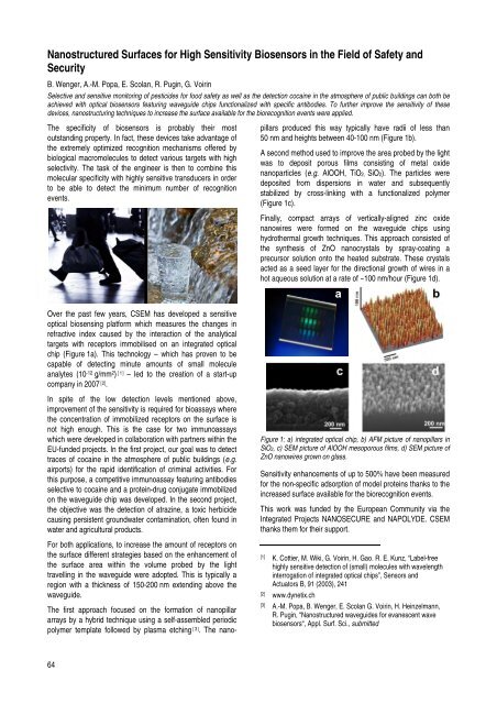
Figure 1: a) integrated optical chip, b) AFM picture of nanopillars in<br />
SiO2, c) SEM picture of AlOOH mesoporous films, d) SEM picture of<br />
ZnO nanowires grown on glass.<br />
Sensitivity enhancements of up to 500% have been measured<br />
for the non-specific adsorption of model proteins thanks to the<br />
increased surface available for the biorecognition events.<br />
This work was funded by the European Community via the<br />
Integrated Projects NANOSECURE <strong>and</strong> NAPOLYDE. <strong>CSEM</strong><br />
thanks them for their support.<br />
[1] K. Cottier, M. Wiki, G. Voirin, H. Gao. R. E. Kunz, “Label-free<br />
highly sensitive detection of (small) molecules with wavelength<br />
interrogation of integrated optical chips”, Sensors <strong>and</strong><br />
Actuators B, 91 (2003), 241<br />
[2] www.dynetix.ch<br />
a<br />
[3] A.-M. Popa, B. Wenger, E. Scolan G. Voirin, H. Heinzelmann,<br />
R. Pugin, “Nanostructured waveguides for evanescent wave<br />
biosensors“, Appl. Surf. Sci., submitted