CSEM Scientific and Technical Report 2008
CSEM Scientific and Technical Report 2008
CSEM Scientific and Technical Report 2008

Create successful ePaper yourself
Turn your PDF publications into a flip-book with our unique Google optimized e-Paper software.
High-speed Imagers<br />
P. Buchschacher, S. Neukom, S. Beer, Y. Zha, Y. Li, R. Cook, T. Baechler<br />
This paper provides insight in the design <strong>and</strong> evaluation of column parallel readout architectures for high speed digital imagers in a 0.18 µm optical<br />
CMOS process.<br />
About 100 years ago, Lucien Bull invented the stereoscopic<br />
spark-drum camera, which took pictures at up to 2’000 frames<br />
per second (fps) <strong>and</strong> was the first machine to analyse the<br />
wing-beats of insects successfully (Figure 1, left). Dr Bull<br />
imprisoned the insect in a glass tube so that, when it flew out,<br />
it lifted up a tiny flap at the exit. This automatically closed the<br />
electrical circuit operating the camera shutter (in effect the<br />
insect was photographing itself).<br />
Figure 1: Left – Lucien Bull with his high-speed (2kfps) camera, Paris,<br />
1904 (Photo: NMEM Science & Society); Right – modern digital highspeed<br />
camera (courtesy AOS Technologies AG)<br />
Electronic image sensors of today can be considered as “highspeed”<br />
as soon as they exceed video rates. The “speed”<br />
(maximum frame rate) of an image sensor is indeed closely<br />
related to its spatial resolution <strong>and</strong> more particularly to its<br />
number of rows. For example, a sensor capable of 1’000 fps<br />
while scanning 1’000 rows (row-rate = 1 µs) is able to deliver<br />
10’000 fps when scanning a partial image of 100 rows (rowrate<br />
=1 µs). The reason why the number of columns has<br />
almost no impact on the sensor frame rate is that the majority<br />
of high-speed sensors nowadays use column parallel readout<br />
circuitry. Up to the 1990’s, CCD- <strong>and</strong> early CIS [ 1] delivered<br />
analog output <strong>and</strong> thus A/D conversion had to be performed in<br />
separate ICs. With the advent in the late 1990s of the first onchip<br />
column-parallel ADCs, the way was paved for<br />
implementing high-speed / high resolution digital imagers.<br />
When this project was started in 2006, a typical high-speed<br />
1.3 Megapixel digital CIS as used in a modern camera<br />
(Figure 1, right) delivered 500 fps at full resolution (row-rate<br />
= 2 µs) <strong>and</strong> needed a companion FPGA to sequence its<br />
operation [2] . The target therefore was to push the speed <strong>and</strong><br />
functionality of such a CIS at a similar performance level as<br />
Bull’s 100 year old bench, namely to sustain 2 kfps at full<br />
resolution (row-rate = 0.5 µs) while integrating useful trigger<br />
supporting functions (a modern ersatz of Bull’s glass-tube flap)<br />
<strong>and</strong> auto-exposure controller on the same die.<br />
In a first step, a partial integration of the sensor main analog<br />
blocks in a 0.18 µm optical process with conventional<br />
photodiodes (Figure 2) was realized. As the 12 µm2 pixel pitch<br />
was requested from the application, well-known 5T snapshoot<br />
pixels [1, 2] for the sensor array were selected. To<br />
increase the column processing throughput, <strong>CSEM</strong> opted for a<br />
two-row-at-a-time / time-interleaved row-addressing scheme.<br />
For the readout circuitry an early low-power architecture [ 3]<br />
which was boosted-up for high-speed operation was re-used.<br />
34<br />
4mm<br />
3mm<br />
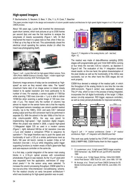
Figure 2: 1 st integration of the analog blocks. Left – test bed;<br />
Right – IC.<br />
The readout was made of data-difference sampling (DDS)<br />
stages with programmable gain <strong>and</strong> 10-bit SAR ADCs running<br />
at four times the row-rate (125 ns / column), as depicted in<br />
Figure 3 left. The evaluation of this 1st integration showed<br />
mixed results: on the one h<strong>and</strong>, the optical characterisation of<br />
the pixel diodes as well as the functionality of the ADCs was<br />
successful, but on the other h<strong>and</strong> the DDS stages did not<br />
work properly.<br />
<strong>CSEM</strong> thus devised a redesign of the readout path, in which<br />
the throughput of the analog blocks to one time the row-rate<br />
(500 ns/column, Figure 3 center) was essentially reduced.<br />
This 2nd chip, which is now in the process of being integrated,<br />
incorporates the full digital functionality of the target 1.3 Mpix<br />
sensor (on-chip sequencer, ROI trigger, exposure controller),<br />
as well as (new) pinned photodiodes for improved sensitivity.<br />
2<br />
8*10<br />
Top readout<br />
Pixel array<br />
DDS DDS<br />
DDS<br />
1<br />
Bottom<br />
readout<br />
1<br />
Bottom<br />
readout<br />
ADC ADC<br />
ADC<br />
10<br />
10<br />
Mux Mux<br />
8*10<br />
8*10<br />
2<br />
DDS<br />
DDS<br />
DDS<br />
DDS<br />
ADC<br />
ADC<br />
ADC<br />
ADC<br />
8*10<br />
Top readout<br />
Pixel array<br />
DDS<br />
DDS<br />
ADC<br />
ADC<br />
10mm<br />
5mm<br />
Figure 3: Left – 1 st readout architecture; Center – 2 nd readout<br />
architecture; Right – 2 nd integration with 256x256 pixel field<br />
This work was partly funded by the CTI/KTI (contract number<br />
8035.2 NMPP-NM). <strong>CSEM</strong> thanks them for their support.<br />
[1] S. Lauxtermann, et al., “A high speed CMOS imager acquiring<br />
5000 frames/sec”, dig. IEDM '99 conf, pp.875-878, December<br />
1999<br />
[2] A. Krymski, et al., “A High Speed, 500 fps, 1024x1024 CMOS<br />
Active Pixel Sensor”, IEEE VLSI Cir. conf., June 1999, 137-138<br />
[3] M. Ansorge, et al., “Smart Low-Power CMOS Cameras for 3G<br />
Mobile Communicators”, proc. IEEE ICSC'02, June 2002, 216-<br />
225