CSEM Scientific and Technical Report 2008
CSEM Scientific and Technical Report 2008
CSEM Scientific and Technical Report 2008

You also want an ePaper? Increase the reach of your titles
YUMPU automatically turns print PDFs into web optimized ePapers that Google loves.
Polarization Imaging using Nanostructured Metal Grids<br />
M. Guillaumée, L. A. Dunbar, C. Santschi, E. Grenet, R. Eckert, R. P. Stanley<br />
Efficient wire grid polarizers have been designed, fabricated <strong>and</strong> characterized on CMOS photodetectors. Placing such polarizers on each pixel of a<br />
CMOS sensor allows the reconstruction of the polarization state, providing additional information on object properties being imaged.<br />
CMOS image sensors are found in many devices, from mobile<br />
phone cameras to high performance industrial sensors. They<br />
are sensitive across the visible, <strong>and</strong> color information can be<br />
extracted through filters on individual pixels. The integration of<br />
micro-polarizers on each individual pixel, in a configuration<br />
similar to the Bayer one (cf. Figure 1), allows the<br />
reconstruction of the polarization state [1] . Polarization imaging<br />
provides information such as shape <strong>and</strong> material properties.<br />
For example, polarization imaging can improve biomedical<br />
imaging contrast due to the birefringence of biological tissue [2] .<br />
In the present work, the integration of wire grid polarizers on<br />
pixels of CMOS photodetectors is achieved.<br />
Figure 1: The Bayer-like arrangement of micro-polarizers on the pixel<br />
array of an image sensor<br />
Metallic wire grids (see Figure 2) are well established as<br />
efficient polarizers (high transmission <strong>and</strong> high extinction ratio),<br />
providing high acceptance angle <strong>and</strong> broadb<strong>and</strong> polarization<br />
extinction ratio (ER). Wire grids are commonly used from<br />
radio-waves to the infrared. Their extension to the visible is<br />
challenging: to obtain both high transmission <strong>and</strong> ER in a wire<br />
grid polarizer, the pitch p of the grid (Figure 2) has to be much<br />
smaller than the incident wavelength λ (p < λ/10), i.e.<br />
p < 100 nm.<br />
Figure 2: A schematic of a wire grid polarizer on a glass substrate<br />
<strong>and</strong> definitions used for the grid dimensions<br />
It would be commercially interesting to fabricate these grids<br />
directly in the CMOS process. The period <strong>and</strong> slit width need<br />
to be compatible with typical CMOS dimensions while<br />
preserving efficient polarization properties. Suitable designs<br />
can be found by optimizing both the aperture width w <strong>and</strong> the<br />
film thickness h. An analytical model was used to underst<strong>and</strong><br />
the physics behind the transmission process of the polarizer.<br />
This model was used to optimize the design of the polarizer,<br />
which <strong>CSEM</strong> was able to demonstrate.<br />
As a first step, metallic gratings are on glass substrates. Good<br />
agreement with theory is observed [3] . A polarization extinction<br />
ratio of around 100 is measured from 600 nm to 900 nm with<br />
p = 500 nm, w = 150 nm <strong>and</strong> h = 285 nm. The gratings also<br />
show high transmission (>60%). Gold gratings with similar<br />
dimensions were fabricated <strong>and</strong> characterized on<br />
photodetectors. An extinction ratio higher than 200 is<br />
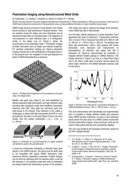
measured (cf. Figure 3), demonstrating the possibility to<br />
integrate efficient metallic gratings on CMOS detectors. The<br />
fringes observed in Figure 3 are due to a Fabry-Pérot effect<br />
due to the silicon oxide layer of several microns above the<br />
active region inherent to the CMOS fabrication process used<br />
for this device.<br />
Figure 3: Extinction ratio measured for a gold grating fabricated on a<br />
CMOS photodetector pixel (p = 500, h = 340 nm <strong>and</strong> w = 150 nm)<br />
This work demonstrates both theoretically <strong>and</strong> experimentally<br />
that it is possible to design efficient metallic grid polarizers<br />
within CMOS process constraints. An array of such polarizers<br />
placed above the pixel array of a CMOS camera would allow<br />
real time polarization imaging. These structures could also be<br />
used for other optical devices such as projection displays.<br />
This work was funded by the European Community, project no.<br />
IST-FP6- 034506 'PLEAS'.<br />
[1] G. P. Nordin, J. T. Meier, P. C. Deguzman, M. W. Jones,<br />
“Micropolarizer array for infrared imaging polarimetry”, J. Opt.<br />
Soc. Am. A, 16 (1999) 1168<br />
[2] S. Makita, Y. Yasuno, T. Endo, M. Itoh, T. Yatagai, “Polarization<br />
contrast imaging of biological tissues by polarization-sensitive<br />
Fourier-domain optical coherence tomography”, Appl. Opt., 45<br />
(2006) 1142<br />
[3] M. Guillaumée, L. A. Dunbar, C. Santschi, E. Grenet, R. Eckert,<br />
R. P. Stanley, “Polarization imaging on CMOS photodetector<br />
using nanostructured metallic grids”, Appl. Phys. Lett., submitted<br />
(2009)<br />
45