CSEM Scientific and Technical Report 2008
CSEM Scientific and Technical Report 2008
CSEM Scientific and Technical Report 2008

Create successful ePaper yourself
Turn your PDF publications into a flip-book with our unique Google optimized e-Paper software.
Batch Fabrication of Ultrathin Nanoporous Membranes<br />
A.-M. Popa, P. Niedermann, R. Pugin<br />
Block-copolymer assisted nanostructuring has been successfully employed for the definition of densely packed nanopores with a mean diameter of<br />
80 nm in silicon nitride thin films with a thickness of 100 nm. The release of these films by st<strong>and</strong>ard microfabrication techniques leads to suspended<br />
nanoporous membranes with areas ranging from 100 to 16000 μm 2 .<br />
Nanoporous membranes are essential components in<br />
ultrafiltration, sensing <strong>and</strong> “smart” cell-culture devices. Most<br />
available systems, however, display poor chemical <strong>and</strong><br />
mechanical stability, broad pore size distribution, <strong>and</strong> a high<br />
aspect ratio of the nanopores (1:1000). These properties<br />
result in fast membrane degradation, poor molecular cut-off,<br />
important material losses, <strong>and</strong> long response times. In order<br />
to overcome these drawbacks <strong>CSEM</strong> has recently developed<br />
processes for the fabrication of mechanically stable ultrathin<br />
silicon nitride membranes with extremely narrow pore size<br />
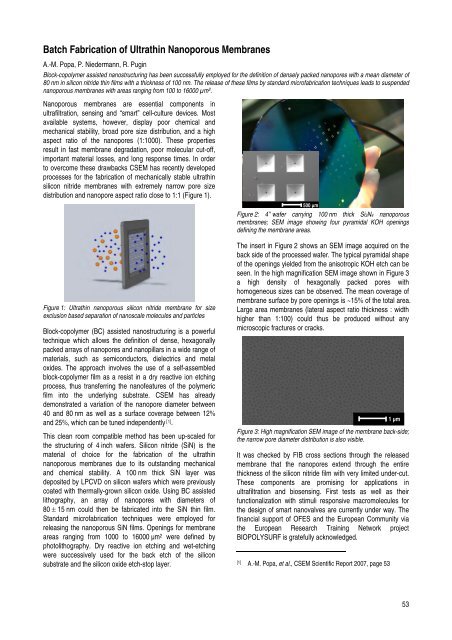
distribution <strong>and</strong> nanopore aspect ratio close to 1:1 (Figure 1).<br />
Figure 1: Ultrathin nanoporous silicon nitride membrane for size<br />
exclusion based separation of nanoscale molecules <strong>and</strong> particles<br />
Block-copolymer (BC) assisted nanostructuring is a powerful<br />
technique which allows the definition of dense, hexagonally<br />
packed arrays of nanopores <strong>and</strong> nanopillars in a wide range of<br />
materials, such as semiconductors, dielectrics <strong>and</strong> metal<br />
oxides. The approach involves the use of a self-assembled<br />
block-copolymer film as a resist in a dry reactive ion etching<br />
process, thus transferring the nanofeatures of the polymeric<br />
film into the underlying substrate. <strong>CSEM</strong> has already<br />
demonstrated a variation of the nanopore diameter between<br />
40 <strong>and</strong> 80 nm as well as a surface coverage between 12%<br />
<strong>and</strong> 25%, which can be tuned independently [1] .<br />
This clean room compatible method has been up-scaled for<br />
the structuring of 4 inch wafers. Silicon nitride (SiN) is the<br />
material of choice for the fabrication of the ultrathin<br />
nanoporous membranes due to its outst<strong>and</strong>ing mechanical<br />
<strong>and</strong> chemical stability. A 100 nm thick SiN layer was<br />
deposited by LPCVD on silicon wafers which were previously<br />
coated with thermally-grown silicon oxide. Using BC assisted<br />
lithography, an array of nanopores with diameters of<br />
80 ± 15 nm could then be fabricated into the SiN thin film.<br />
St<strong>and</strong>ard microfabrication techniques were employed for<br />
releasing the nanoporous SiN films. Openings for membrane<br />
areas ranging from 1000 to 16000 μm 2 were defined by<br />
photolithography. Dry reactive ion etching <strong>and</strong> wet-etching<br />
were successively used for the back etch of the silicon<br />
substrate <strong>and</strong> the silicon oxide etch-stop layer.<br />
500 μm<br />
Figure 2: 4’’ wafer carrying 100 nm thick Si3N4 nanoporous<br />
membranes; SEM image showing four pyramidal KOH openings<br />
defining the membrane areas.<br />
The insert in Figure 2 shows an SEM image acquired on the<br />
back side of the processed wafer. The typical pyramidal shape<br />
of the openings yielded from the anisotropic KOH etch can be<br />
seen. In the high magnification SEM image shown in Figure 3<br />
a high density of hexagonally packed pores with<br />
homogeneous sizes can be observed. The mean coverage of<br />
membrane surface by pore openings is ~15% of the total area.<br />
Large area membranes (lateral aspect ratio thickness : width<br />
higher than 1:100) could thus be produced without any<br />
microscopic fractures or cracks.<br />
Figure 3: High magnification SEM image of the membrane back-side;<br />
the narrow pore diameter distribution is also visible.<br />
It was checked by FIB cross sections through the released<br />
membrane that the nanopores extend through the entire<br />
thickness of the silicon nitride film with very limited under-cut.<br />
These components are promising for applications in<br />
ultrafiltration <strong>and</strong> biosensing. First tests as well as their<br />
functionalization with stimuli responsive macromolecules for<br />
the design of smart nanovalves are currently under way. The<br />
financial support of OFES <strong>and</strong> the European Community via<br />
the European Research Training Network project<br />
BIOPOLYSURF is gratefully acknowledged.<br />
[1] A.-M. Popa, et al., <strong>CSEM</strong> <strong>Scientific</strong> <strong>Report</strong> 2007, page 53<br />
1 μm<br />
53