CSEM Scientific and Technical Report 2008
CSEM Scientific and Technical Report 2008
CSEM Scientific and Technical Report 2008

You also want an ePaper? Increase the reach of your titles
YUMPU automatically turns print PDFs into web optimized ePapers that Google loves.
Packaging Technology for Silicon Resonators<br />
J. Baborowski, A. Pezous, C. Muller, G. Spinola Durante, M.-A. Dubois<br />
Recently, two types of Low Frequency silicon resonators with AlN piezoelectric activation have been developed. Whatever the type of resonator, its<br />
properties are enhanced when operated under vacuum. The main motivation for the packaging of resonator under vacuum is to increase the<br />
Q factor, <strong>and</strong> to guarantee a long-term stability for frequency reference. In order to minimize the size of packaged resonators, wafer level packaging<br />
(WLP) is the right option. WLP also offers other opportunities for further integration of RF MEMS <strong>and</strong> IC components.<br />
Hermetic packaging at low pressure is one of the largest<br />
barriers to commercialisation of MEMS timing reference. In<br />
this project the solutions for WLP of the resonator have been<br />
demonstrated.<br />
Packaging of resonators consists in building a hermetic cavity<br />
around the resonator. This is done in three steps (Figure 1):<br />
1. Fabrication of the AlN/Si resonator<br />
2. Wafer-to-Wafer rear side packaging<br />
3. Die-to-die front-side packaging performed under vacuum.<br />
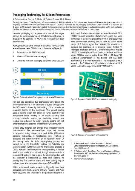
Figure 1: Schematic view of packaging principle for AlN/Si resonators<br />
For rear side packaging, two approaches were tested. The<br />
first solution consists in the fabrication of buried cavities within<br />
the SOI wafer, followed by the building of the piezoelectric<br />
resonator directly on the membrane. The second solution<br />
uses a capping wafer (thin silicon or Pyrex) sealed by low<br />
temperature fusion bonding or by anodic bonding. Both<br />
bonding methods require an extremely smooth <strong>and</strong><br />
residue-free surface of the wafer. Hermetic sealing with high<br />
shear strength was obtained for resonator/Pyrex s<strong>and</strong>wich.<br />
Metallic alloy materials can provide low-permeability sealing<br />
characteristics. The resonator/Pyrex chips are vacuum<br />
encapsulated using silicon caps <strong>and</strong> AuSn (80% wt Au)<br />
soldering technology. A metallization layer (TiW-Au) is<br />
deposited <strong>and</strong> patterned (lift-off) on the resonator wafer. On<br />
the capping wafer the AuSn electroplating process was<br />
carried out at the Fraunhofer Institute for Reliability <strong>and</strong><br />
Microintegration (IZM FhG) <strong>and</strong> the final sealing process at<br />
<strong>CSEM</strong> Alpnach. The quality of the sealing resulting in vacuum<br />
level in the cavity is monitored through measurements of<br />
resonator Q factor. In this version, the electrical contact with<br />
the resonator is established via metal lines crossing the<br />
sealing ring. The electrical signal <strong>and</strong> metal sealing ring are<br />
isolated by an adequate passivation layer (SiO2 or SiON).<br />
1 MHz extensional mode resonators (Figure 2) have been<br />
packaged using thin Si capping (200 μm, Figure 3) <strong>and</strong> Pyrex<br />
wafer (300 μm). The total size of the packaged resonator is<br />
28<br />
3<br />
1<br />
2<br />
top cap<br />
resonator<br />
bottom cap<br />
4x3x1 mm 3 . Further miniaturization can be achieved with 32 to<br />
120 kHz flexural resonators (2x2x0.6 mm 3 ) using the same<br />
technology. In a previous project the effect of air pressure has<br />
been demonstrated showing that in order to obtain stable<br />
values of Q factors higher than 100000 it is m<strong>and</strong>atory to<br />
maintain the resonator at a pressure below 1 mbar [ 1] .<br />
Packaged resonators exhibit a Q factor in vacuum as high as<br />
140000, a coupling factor k 2 eff of 0.06%, a motional resistance<br />
below 200 Ohm <strong>and</strong> a mainly linear TCf of -28.5 ppm/°C.<br />
Electronic compensation of this thermal drift has been<br />
demonstrated in the MIP Packtime [2] . The integration of WLP<br />
resonator, BAW filters <strong>and</strong> IC to build a miniaturized ULP<br />
MEMS radio is the scope of the EU IP “MINAmI” [3] .<br />
Figure 2: Top view of 1MHz AlN/Si resonators with sealing ring<br />
Figure 3: Top view of capping die with sealing ring<br />
[1] J. Baborowski, et al., “Silicon Resonators: Thermal<br />
Compensation <strong>and</strong> Q Factor Optimization”, <strong>CSEM</strong> <strong>Scientific</strong><br />
<strong>Report</strong> 2007, page 9<br />
[2] D. Ruffieux, et al., “PackTime: Zero-Level Packaging of Silicon<br />
Time-base for RTC <strong>and</strong> Reference Frequency Applications”, in<br />
this report, page 10<br />
[3] http://www.fp6-minami.org