
Create successful ePaper yourself
Turn your PDF publications into a flip-book with our unique Google optimized e-Paper software.
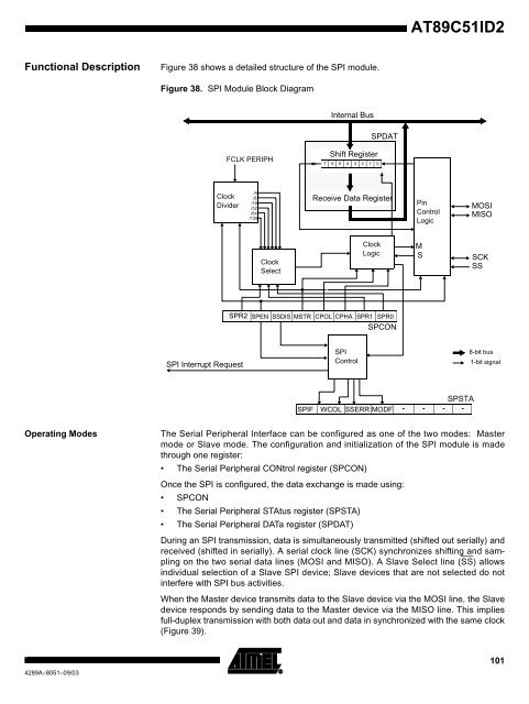
Functional Description Figure 38 shows a detailed structure of the SPI module.<br />
4289A–8051–09/03<br />
Figure 38. SPI Module Block Diagram<br />
Clock<br />
Divider<br />
SPI Interrupt Request<br />
FCLK PERIPH<br />
/4<br />
/8<br />
/16<br />
/32<br />
/64<br />
/128<br />
Clock<br />
Select<br />
SPR2 SPEN SSDIS MSTR CPOL<br />
Shift Register<br />
<strong>AT89C51ID2</strong><br />
Operating Modes The Serial Peripheral Interface can be configured as one of the two modes: Master<br />
mode or Slave mode. The configuration and initialization of the SPI module is made<br />
through one register:<br />
The Serial Peripheral CONtrol register (SPCON)<br />
Once the SPI is configured, the data exchange is made using:<br />
SPCON<br />
The Serial Peripheral STAtus register (SPSTA)<br />
The Serial Peripheral DATa register (SPDAT)<br />
During an SPI transmission, data is simultaneously transmitted (shifted out serially) and<br />
received (shifted in serially). A serial clock line (SCK) synchronizes shifting and sampling<br />
on the two serial data lines (MOSI and MISO). A Slave Select line (SS) allows<br />
individual selection of a Slave SPI device; Slave devices that are not selected do not<br />
interfere with SPI bus activities.<br />
When the Master device transmits data to the Slave device via the MOSI line, the Slave<br />
device responds by sending data to the Master device via the MISO line. This implies<br />
full-duplex transmission with both data out and data in synchronized with the same clock<br />
(Figure 39).<br />
7<br />
Internal Bus<br />
6<br />
5<br />
4<br />
Receive <strong>Data</strong> Register<br />
3<br />
SPI<br />
Control<br />
2<br />
1<br />
SPDAT<br />
0<br />
Clock<br />
Logic<br />
CPHA SPR1 SPR0<br />
SPCON<br />
Pin<br />
Control<br />
Logic<br />
SPIF WCOL SSERR<br />
MODF - - -<br />
SPSTA<br />
-<br />
M<br />
S<br />
MOSI<br />
MISO<br />
SCK<br />
SS<br />
8-bit bus<br />
1-bit signal<br />
101