
Create successful ePaper yourself
Turn your PDF publications into a flip-book with our unique Google optimized e-Paper software.
102 <strong>AT89C51ID2</strong><br />
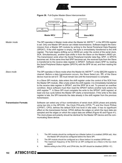
Figure 39. Full-Duplex Master-Slave Interconnection<br />
SPI<br />
Clock Generator<br />
8-bit Shift register<br />
Master MCU<br />
8-bit Shift register<br />
Master mode The SPI operates in Master mode when the Master bit, MSTR (1) , in the SPCON register<br />
is set. Only one Master SPI device can initiate transmissions. Software begins the transmission<br />
from a Master SPI module by writing to the Serial Peripheral <strong>Data</strong> Register<br />
(SPDAT). If the shift register is empty, the byte is immediately transferred to the shift<br />
register. The byte begins shifting out on MOSI pin under the control of the serial clock,<br />
SCK. Simultaneously, another byte shifts in from the Slave on the Master’s MISO pin.<br />
The transmission ends when the Serial Peripheral transfer data flag, SPIF, in SPSTA<br />
becomes set. At the same time that SPIF becomes set, the received byte from the Slave<br />
is transferred to the receive data register in SPDAT. Software clears SPIF by reading<br />
the Serial Peripheral Status register (SPSTA) with the SPIF bit set, and then reading the<br />
SPDAT.<br />
Slave mode The SPI operates in Slave mode when the Master bit, MSTR (2) , in the SPCON register is<br />
cleared. Before a data transmission occurs, the Slave Select pin, SS, of the Slave<br />
device must be set to’0’. SS must remain low until the transmission is complete.<br />
In a Slave SPI module, data enters the shift register under the control of the SCK from<br />
the Master SPI module. After a byte enters the shift register, it is immediately transferred<br />
to the receive data register in SPDAT, and the SPIF bit is set. To prevent an overflow<br />
condition, Slave software must then read the SPDAT before another byte enters the<br />
shift register (3) . A Slave SPI must complete the write to the SPDAT (shift register) at<br />
least one bus cycle before the Master SPI starts a transmission. If the write to the data<br />
register is late, the SPI transmits the data already in the shift register from the previous<br />
transmission.<br />
Transmission Formats Software can select any of four combinations of serial clock (SCK) phase and polarity<br />
using two bits in the SPCON: the Clock POLarity (CPOL (4) ) and the Clock PHAse<br />
(CPHA 4 ). CPOL defines the default SCK line level in idle state. It has no significant<br />
effect on the transmission format. CPHA defines the edges on which the input data are<br />
sampled and the edges on which the output data are shifted (Figure 40 and Figure 41).<br />
The clock phase and polarity should be identical for the Master SPI device and the communicating<br />
Slave device.<br />
MISO<br />
MOSI<br />
MISO<br />
MOSI<br />
SCK SCK<br />
SS<br />
VDD<br />
SS<br />
VSS<br />
Slave MCU<br />
1. The SPI module should be configured as a Master before it is enabled (SPEN set). Also<br />
the Master SPI should be configured before the Slave SPI.<br />
2. The SPI module should be configured as a Slave before it is enabled (SPEN set).<br />
3. The maximum frequency of the SCK for an SPI configured as a Slave is the bus clock<br />
speed.<br />
4. Before writing to the CPOL and CPHA bits, the SPI should be disabled (SPEN =’0’).<br />
4289A–8051–09/03