You also want an ePaper? Increase the reach of your titles
YUMPU automatically turns print PDFs into web optimized ePapers that Google loves.
30 <strong>AT89C51ID2</strong><br />
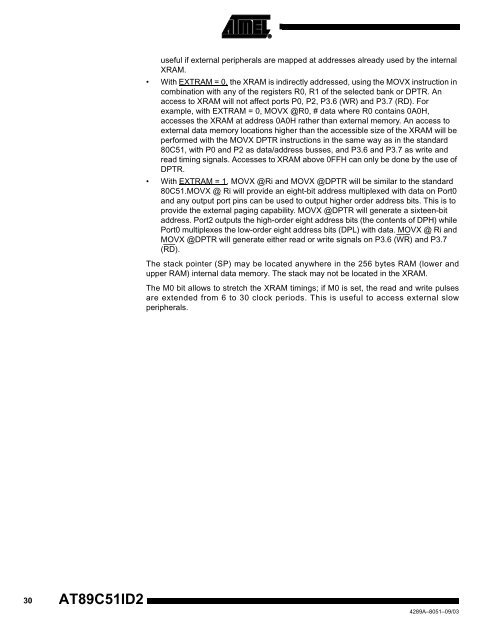
useful if external peripherals are mapped at addresses already used by the internal<br />
XRAM.<br />
With EXTRAM = 0, the XRAM is indirectly addressed, using the MOVX instruction in<br />
combination with any of the registers R0, R1 of the selected bank or DPTR. An<br />
access to XRAM will not affect ports P0, P2, P3.6 (WR) and P3.7 (RD). For<br />
example, with EXTRAM = 0, MOVX @R0, # data where R0 contains 0A0H,<br />
accesses the XRAM at address 0A0H rather than external memory. An access to<br />
external data memory locations higher than the accessible size of the XRAM will be<br />
performed with the MOVX DPTR instructions in the same way as in the standard<br />
80C51, with P0 and P2 as data/address busses, and P3.6 and P3.7 as write and<br />
read timing signals. Accesses to XRAM above 0FFH can only be done by the use of<br />
DPTR.<br />
With EXTRAM = 1 , MOVX @Ri and MOVX @DPTR will be similar to the standard<br />
80C51.MOVX @ Ri will provide an eight-bit address multiplexed with data on Port0<br />
and any output port pins can be used to output higher order address bits. This is to<br />
provide the external paging capability. MOVX @DPTR will generate a sixteen-bit<br />
address. Port2 outputs the high-order eight address bits (the contents of DPH) while<br />
Port0 multiplexes the low-order eight address bits (DPL) with data. MOVX @ Ri and<br />
MOVX @DPTR will generate either read or write signals on P3.6 (WR) and P3.7<br />
(RD).<br />
The stack pointer (SP) may be located anywhere in the 256 bytes RAM (lower and<br />
upper RAM) internal data memory. The stack may not be located in the XRAM.<br />
The M0 bit allows to stretch the XRAM timings; if M0 is set, the read and write pulses<br />
are extended from 6 to 30 clock periods. This is useful to access external slow<br />
peripherals.<br />
4289A–8051–09/03


