
You also want an ePaper? Increase the reach of your titles
YUMPU automatically turns print PDFs into web optimized ePapers that Google loves.
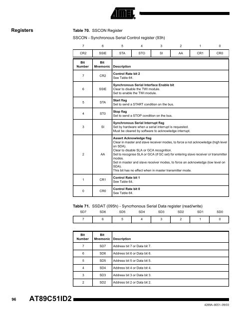
Registers Table 70. SSCON Register<br />
SSCON - Synchronous Serial Control register (93h)<br />
96 <strong>AT89C51ID2</strong><br />
7 6 5 4 3 2 1 0<br />
CR2 SSIE STA STO SI AA CR1 CR0<br />
Bit<br />
Number<br />
Bit<br />
Mnemonic Description<br />
7 CR2<br />
6 SSIE<br />
5 STA<br />
4 ST0<br />
3 SI<br />
2 AA<br />
1 CR1<br />
0 CR0<br />
Control Rate bit 2<br />
See Table 64.<br />
Synchronous Serial Interface Enable bit<br />
Clear to disable the TWI module.<br />
Set to enable the TWI module.<br />
Start flag<br />
Set to send a START condition on the bus.<br />
Stop flag<br />
Set to send a STOP condition on the bus.<br />
Synchronous Serial Interrupt flag<br />
Set by hardware when a serial interrupt is requested.<br />
Must be cleared by software to acknowledge interrupt.<br />
Assert Acknowledge flag<br />
Clear in master and slave receiver modes, to force a not acknowledge (high level<br />
on SDA).<br />
Clear to disable SLA or GCA recognition.<br />
Set to recognise SLA or GCA (if GC set) for entering slave receiver or transmitter<br />
modes.<br />
Set in master and slave receiver modes, to force an acknowledge (low level on<br />
SDA).<br />
This bit has no effect when in master transmitter mode.<br />
Control Rate bit 1<br />
See Table 64.<br />
Control Rate bit 0<br />
See Table 64.<br />
Table 71. SSDAT (095h) - Syncrhonous Serial <strong>Data</strong> register (read/write)<br />
SD7 SD6 SD5 SD4 SD3 SD2 SD1 SD0<br />
7 6 5 4 3 2 1 0<br />
Bit<br />
Number<br />
Bit<br />
Mnemonic Description<br />
7 SD7 Address bit 7 or <strong>Data</strong> bit 7.<br />
6 SD6 Address bit 6 or <strong>Data</strong> bit 6.<br />
5 SD5 Address bit 5 or <strong>Data</strong> bit 5.<br />
4 SD4 Address bit 4 or <strong>Data</strong> bit 4.<br />
3 SD3 Address bit 3 or <strong>Data</strong> bit 3.<br />
2 SD2 Address bit 2 or <strong>Data</strong> bit 2.<br />
4289A–8051–09/03