
Create successful ePaper yourself
Turn your PDF publications into a flip-book with our unique Google optimized e-Paper software.
T A = -40°C to +85°C; V SS = 0V; V CC =2.7V to 5.5V; F = 0 to 60 MHz (Continued)<br />
4289A–8051–09/03<br />
<strong>AT89C51ID2</strong><br />
Symbol Parameter Min Typ Max Unit Test Conditions<br />
R RST RST Pull-down Resistor 50 200 (5)<br />
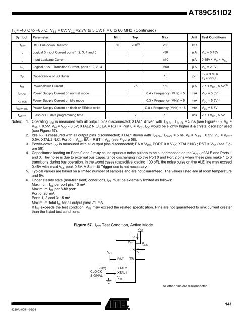
Notes: 1. Operating I CC is measured with all output pins disconnected; XTAL1 driven with T CLCH , T CHCL = 5 ns (see Figure 60), V IL =<br />
V SS + 0.5V, V IH = V CC - 0.5V; XTAL2 N.C.; EA = RST = Port 0 = V CC . I CC would be slightly higher if a crystal oscillator used<br />
(see Figure 57).<br />
2. Idle I CC is measured with all output pins disconnected; XTAL1 driven with T CLCH , T CHCL = 5 ns, V IL = V SS + 0.5V, V IH = V CC -<br />
0.5V; XTAL2 N.C; Port 0 = V CC ; EA = RST = V SS (see Figure 58).<br />
3. Power-down I CC is measured with all output pins disconnected; EA = V CC , PORT 0 = V CC ; XTAL2 NC.; RST = V SS (see Figure<br />
59).<br />
4. Capacitance loading on Ports 0 and 2 may cause spurious noise pulses to be superimposed on the V OLS of ALE and Ports 1<br />
and 3. The noise is due to external bus capacitance discharging into the Port 0 and Port 2 pins when these pins make 1 to 0<br />
transitions during bus operation. In the worst cases (capacitive loading 100 pF), the noise pulse on the ALE line may exceed<br />
0.45V with maxi V OL peak 0.6V. A Schmitt Trigger use is not necessary.<br />
5. Typical values are based on a limited number of samples and are not guaranteed. The values listed are at room temperature<br />
and 5V.<br />
6. Under steady state (non-transient) conditions, I OL must be externally limited as follows:<br />
Maximum I OL per port pin: 10 mA<br />
Maximum I OL per 8-bit port:<br />
Port 0: 26 mA<br />
Ports 1, 2 and 3: 15 mA<br />
Maximum total I OL for all output pins: 71 mA<br />
If I OL exceeds the test condition, V OL may exceed the related specification. Pins are not guaranteed to sink current greater<br />
than the listed test conditions.<br />
Figure 57. I CC Test Condition, Active Mode<br />
250 kΩ<br />
I IL Logical 0 Input Current ports 1, 2, 3, 4 and 5 -50 µA V IN = 0.45V<br />
I LI Input Leakage Current ±10 µA 0.45V < V IN < V CC<br />
I TL Logical 1 to 0 Transition Current, ports 1, 2, 3, 4 -650 µA V IN = 2.0V<br />
C IO Capacitance of I/O Buffer 10 pF<br />
F C = 3 MHz<br />
T A = 25°C<br />
I PD Power-down Current 75 150 µA 2.7 < V CC < 5.5V (3)<br />
I CCOP Power Supply Current on normal mode 0.4 x Frequency (MHz) + 5 mA V CC = 5.5V (1)<br />
I CCIDLE Power Supply Current on idle mode 0.3 x Frequency (MHz) + 5 mA V CC = 5.5V (2)<br />
I CCWRITE Power Supply Current on flash or EEdata write 0.8 x Frequency (MHz) + 15 mA V CC = 5.5V<br />
t WRITE Flash or EEdata programming time 7 10 ms 2.7 < V CC < 5.5V<br />
(NC)<br />
CLOCK<br />
SIGNAL<br />
V CC<br />
RST<br />
XTAL2<br />
XTAL1<br />
V SS<br />
V CC<br />
I CC<br />
P0<br />
EA<br />
V CC<br />
V CC<br />
All other pins are disconnected.<br />
141