
Create successful ePaper yourself
Turn your PDF publications into a flip-book with our unique Google optimized e-Paper software.
Flash Registers and<br />
Memory Map<br />
118 <strong>AT89C51ID2</strong><br />
The <strong>AT89C51ID2</strong> Flash memory uses several registers for his management:<br />
Hardware registers can only be accessed through the parallel programming modes<br />
which are handled by the parallel programmer.<br />
Software registers are in a special page of the Flash memory which can be<br />
accessed through the API or with the parallel programming modes. This page,<br />
called "Extra Flash Memory", is not in the internal Flash program memory<br />
addressing space.<br />
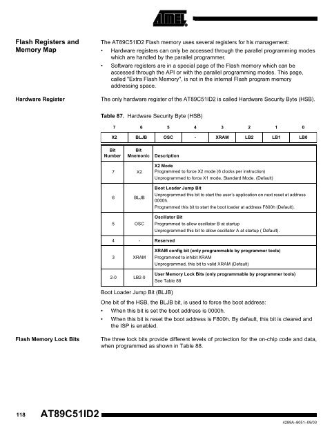
Hardware Register The only hardware register of the <strong>AT89C51ID2</strong> is called Hardware Security Byte (HSB).<br />
Table 87. Hardware Security Byte (HSB)<br />
7 6 5 4 3 2 1 0<br />
X2 BLJB OSC - XRAM LB2 LB1 LB0<br />
Bit<br />
Number<br />
Bit<br />
Mnemonic Description<br />
7 X2<br />
6 BLJB<br />
5 OSC<br />
4 - Reserved<br />
3 XRAM<br />
2-0 LB2-0<br />
X2 Mode<br />
Programmed to force X2 mode (6 clocks per instruction)<br />
Unprogrammed to force X1 mode, Standard Mode. (Default)<br />
Boot Loader Jump Bit<br />
Unprogrammed this bit to start the user’s application on next reset at address<br />
0000h.<br />
Programmed this bit to start the boot loader at address F800h (Default).<br />
Oscillator Bit<br />
Programmed to allow oscillator B at startup<br />
Unprogrammed this bit to allow oscillator A at startup ( Default).<br />
XRAM config bit (only programmable by programmer tools)<br />
Programmed to inhibit XRAM<br />
Unprogrammed, this bit to valid XRAM (Default)<br />
User Memory Lock Bits (only programmable by programmer tools)<br />
See Table 88<br />
Boot Loader Jump Bit (BLJB)<br />
One bit of the HSB, the BLJB bit, is used to force the boot address:<br />
When this bit is set the boot address is 0000h.<br />
When this bit is reset the boot address is F800h. By default, this bit is cleared and<br />
the ISP is enabled.<br />
Flash Memory Lock Bits The three lock bits provide different levels of protection for the on-chip code and data,<br />
when programmed as shown in Table 88.<br />
4289A–8051–09/03