
You also want an ePaper? Increase the reach of your titles
YUMPU automatically turns print PDFs into web optimized ePapers that Google loves.
Serial Port Interface<br />
(SPI)<br />
4289A–8051–09/03<br />
<strong>AT89C51ID2</strong><br />
The Serial Peripheral Interface module (SPI) allows full-duplex, synchronous, serial<br />
communication between the MCU and peripheral devices, including other MCUs.<br />
Features Features of the SPI module include the following:<br />
Full-duplex, three-wire synchronous transfers<br />
Master or Slave operation<br />
Eight programmable Master clock rates<br />
Serial clock with programmable polarity and phase<br />
Master Mode fault error flag with MCU interrupt capability<br />
Write collision flag protection<br />
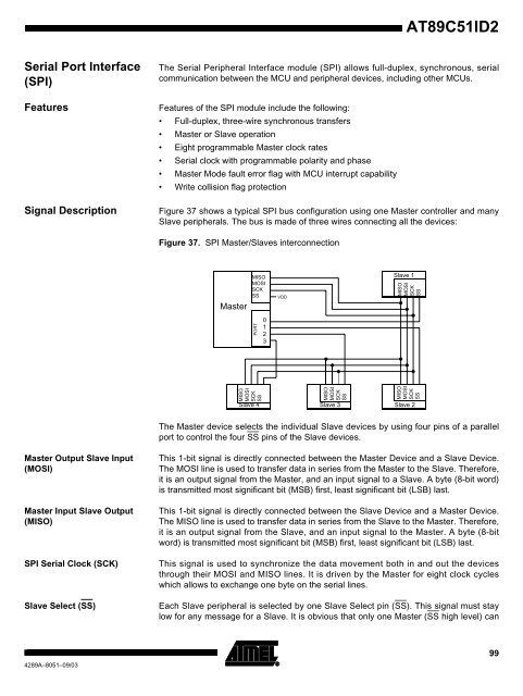
Signal Description Figure 37 shows a typical SPI bus configuration using one Master controller and many<br />
Slave peripherals. The bus is made of three wires connecting all the devices:<br />
Master Output Slave Input<br />
(MOSI)<br />
Master Input Slave Output<br />
(MISO)<br />
Figure 37. SPI Master/Slaves interconnection<br />
Master<br />
MISO<br />
MOSI<br />
SCK<br />
SS<br />
PORT<br />
MISO<br />
MOSI<br />
SCK<br />
SS<br />
Slave 4<br />
0<br />
1<br />
2<br />
3<br />
MISO<br />
MOSI<br />
SCK<br />
SS<br />
The Master device selects the individual Slave devices by using four pins of a parallel<br />
port to control the four SS pins of the Slave devices.<br />
This 1-bit signal is directly connected between the Master Device and a Slave Device.<br />
The MOSI line is used to transfer data in series from the Master to the Slave. Therefore,<br />
it is an output signal from the Master, and an input signal to a Slave. A byte (8-bit word)<br />
is transmitted most significant bit (MSB) first, least significant bit (LSB) last.<br />
This 1-bit signal is directly connected between the Slave Device and a Master Device.<br />
The MISO line is used to transfer data in series from the Slave to the Master. Therefore,<br />
it is an output signal from the Slave, and an input signal to the Master. A byte (8-bit<br />
word) is transmitted most significant bit (MSB) first, least significant bit (LSB) last.<br />
SPI Serial Clock (SCK) This signal is used to synchronize the data movement both in and out the devices<br />
through their MOSI and MISO lines. It is driven by the Master for eight clock cycles<br />
which allows to exchange one byte on the serial lines.<br />
Slave Select (SS) Each Slave peripheral is selected by one Slave Select pin (SS). This signal must stay<br />
low for any message for a Slave. It is obvious that only one Master (SS high level) can<br />
VDD<br />
Slave 3<br />
Slave 1<br />
MISO<br />
MOSI<br />
SCK<br />
SS<br />
MISO<br />
MOSI<br />
SCK<br />
SS<br />
Slave 2<br />
99