
You also want an ePaper? Increase the reach of your titles
YUMPU automatically turns print PDFs into web optimized ePapers that Google loves.
4289A–8051–09/03<br />
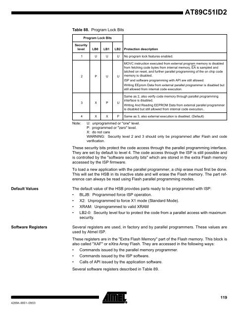
Table 88. Program Lock Bits<br />
Program Lock Bits<br />
Security<br />
level LB0 LB1 LB2<br />
Protection description<br />
1 U U U No program lock features enabled.<br />
2 P U U<br />
3 X P U<br />
<strong>AT89C51ID2</strong><br />
MOVC instruction executed from external program memory is disabled<br />
from fetching code bytes from internal memory, EA is sampled and<br />
latched on reset, and further parallel programming of the on chip code<br />
memory is disabled.<br />
ISP and software programming with API are still allowed.<br />
Writing EEprom <strong>Data</strong> from external parallel programmer is disabled but<br />
still allowed from internal code execution.<br />
Same as 2, also verify code memory through parallel programming<br />
interface is disabled.<br />
Writing And Reading EEPROM <strong>Data</strong> from external parallel programmer<br />
is disabled but still allowed from internal code execution..<br />
4 X X P Same as 3, also external execution is disabled. (Default)<br />
Note: U: unprogrammed or "one" level.<br />
P: programmed or "zero" level.<br />
X: do not care<br />
WARNING: Security level 2 and 3 should only be programmed after Flash and code<br />
verification.<br />
These security bits protect the code access through the parallel programming interface.<br />
They are set by default to level 4. The code access through the ISP is still possible and<br />
is controlled by the "software security bits" which are stored in the extra Flash memory<br />
accessed by the ISP firmware.<br />
To load a new application with the parallel programmer, a chip erase must first be done.<br />
This will set the HSB in its inactive state and will erase the Flash memory. The part reference<br />
can always be read using Flash parallel programming modes.<br />
Default Values The default value of the HSB provides parts ready to be programmed with ISP:<br />
BLJB: Programmed force ISP operation.<br />
X2: Unprogrammed to force X1 mode (Standard Mode).<br />
XRAM: Unprogrammed to valid XRAM<br />
LB2-0: Security level four to protect the code from a parallel access with maximum<br />
security.<br />
Software Registers Several registers are used, in factory and by parallel programmers. These values are<br />
used by <strong>Atmel</strong> ISP.<br />
These registers are in the "Extra Flash Memory" part of the Flash memory. This block is<br />
also called "XAF" or eXtra Array Flash. They are accessed in the following ways:<br />
Commands issued by the parallel memory programmer.<br />
Commands issued by the ISP software.<br />
Calls of API issued by the application software.<br />
Several software registers described in Table 89.<br />
119