- Page 2 and 3:
1 Introduction 1.1 THE ELECTRICAL/E
- Page 4 and 5:
� S I mind that similar progressi
- Page 6 and 7:
� S I denser, which we refer to t
- Page 8 and 9:
� S I decades will probably conta
- Page 10 and 11:
� S I TABLE 1.1 Comparison of the
- Page 12 and 13:
� S I The second was originally d
- Page 14 and 15:
� S I A quick method of determini
- Page 16 and 17:
� S I revealing that the operatio
- Page 18 and 19:
� S I 1 1 2300 � � 3.333E�1
- Page 20 and 21:
� S I Since the power of ten will
- Page 22 and 23:
� S I EXAMPLE 1.14 a. Determine t
- Page 24 and 25:
� S I Initial Settings Format and
- Page 26 and 27:
� S I c. Since the division will
- Page 28 and 29:
� S I Three software packages wil
- Page 30 and 31:
� S I SECTION 1.8 Conversion with
- Page 32 and 33:
2 Current and Voltage 2.1 ATOMS AND
- Page 34 and 35:
I e V CURRENT ⏐⏐⏐ 33 the dist
- Page 36 and 37:
I e V The chemical activity of the
- Page 38 and 39:
I e V erence plane. If the weight i
- Page 40 and 41:
I e V 2.4 FIXED (dc) SUPPLIES The t
- Page 42 and 43:
I e V FIG. 2.14 Maintenance-free 12
- Page 44 and 45:
I e V batteries are relatively warm
- Page 46 and 47:
I e V EXAMPLE 2.5 a. Determine the
- Page 48 and 49:
I e V TABLE 2.1 Relative conductivi
- Page 50 and 51:
I e V be accomplished is to open th
- Page 52 and 53:
I e V (a) (c) Contact Sliding switc
- Page 54 and 55:
I e V Control switch Meter leads (a
- Page 56 and 57:
I e V tant to disconnect the charge
- Page 58 and 59:
I e V GLOSSARY ⏐⏐⏐ 57 28. Fin
- Page 60 and 61:
3 Resistance 3.1 INTRODUCTION The f
- Page 62 and 63:
R G Note that the area of the condu
- Page 64 and 65:
R G EXAMPLE 3.3 What is the resista
- Page 66 and 67:
R G RESISTANCE: METRIC UNITS ⏐⏐
- Page 68 and 69:
R G The conversion factor between r
- Page 70 and 71:
R G Absolute zero -273.15°C Inferr
- Page 72 and 73:
R G Since R 20 of Eq. (3.8) is the
- Page 74 and 75:
R G result is a tremendous saving i
- Page 76 and 77:
R G TYPES OF RESISTORS ⏐⏐⏐ 75
- Page 78 and 79:
R G TYPES OF RESISTORS ⏐⏐⏐ 77
- Page 80 and 81:
R G a 1% failure rate would reveal
- Page 82 and 83:
R G gaps. Dropping to the 10% level
- Page 84 and 85:
R G THERMISTORS ⏐⏐⏐ 83 Prelim
- Page 86 and 87:
R G APPLICATIONS ⏐⏐⏐ 85 3.14
- Page 88 and 89:
R G longer heating element in stand
- Page 90 and 91:
R G cally this law relates voltage,
- Page 92 and 93:
R G MATHCAD ⏐⏐⏐ 91 key at the
- Page 94 and 95:
R G *13. What is the new resistance
- Page 96:
R G SECTION 3.13 Varistors 58. a. R
- Page 99 and 100:
98 ⏐⏐⏐ OHM’S LAW, POWER, AN
- Page 101 and 102:
100 ⏐⏐⏐ OHM’S LAW, POWER, A
- Page 103 and 104:
102 ⏐⏐⏐ OHM’S LAW, POWER, A
- Page 105 and 106:
104 ⏐⏐⏐ OHM’S LAW, POWER, A
- Page 107 and 108:
106 ⏐⏐⏐ OHM’S LAW, POWER, A
- Page 109 and 110:
108 ⏐⏐⏐ OHM’S LAW, POWER, A
- Page 111 and 112:
110 ⏐⏐⏐ OHM’S LAW, POWER, A
- Page 113 and 114:
112 ⏐⏐⏐ OHM’S LAW, POWER, A
- Page 115 and 116:
114 ⏐⏐⏐ OHM’S LAW, POWER, A
- Page 117 and 118:
116 ⏐⏐⏐ OHM’S LAW, POWER, A
- Page 119 and 120:
118 ⏐⏐⏐ OHM’S LAW, POWER, A
- Page 121 and 122:
120 ⏐⏐⏐ OHM’S LAW, POWER, A
- Page 123 and 124:
122 ⏐⏐⏐ OHM’S LAW, POWER, A
- Page 125 and 126:
124 ⏐⏐⏐ OHM’S LAW, POWER, A
- Page 127 and 128:
126 ⏐⏐⏐ OHM’S LAW, POWER, A
- Page 130 and 131:
5 Series Circuits 5.1 INTRODUCTION
- Page 132 and 133:
S the same through series elements
- Page 134 and 135:
S Solution: RT � R1 � R2 � R3
- Page 136 and 137:
S type of element. In other words,
- Page 138 and 139:
S c. V1 � IR1 � (2 A)(4 �)
- Page 140 and 141:
S In the above discussion the curre
- Page 142 and 143:
S Voltage Sources and Ground Except
- Page 144 and 145:
S EXAMPLE 5.14 Find the voltage Vab
- Page 146 and 147:
S EXAMPLE 5.19 Using the voltage di
- Page 148 and 149:
S ∆V L 120 V 100 V 0 V L voltage
- Page 150 and 151:
S EXAMPLE 5.24 Determine the voltag
- Page 152 and 153:
S 5.11 APPLICATIONS Holiday Lights
- Page 154 and 155:
S wiring, you will find that since
- Page 156 and 157:
S and right-click on the mouse. A l
- Page 158 and 159:
S FIG. 5.68 Applying Electronics Wo
- Page 160 and 161:
S also be used to remind the progra
- Page 162 and 163:
S 3. Find the applied voltage E nec
- Page 164 and 165:
S 9. Determine the current I and th
- Page 166 and 167:
S 40 V I + R 3 R 2 R 1 V 3 - 30 �
- Page 168 and 169:
S *28. For the network of Fig. 5.97
- Page 170 and 171:
6 Parallel Circuits 6.1 INTRODUCTIO
- Page 172 and 173:
P rent level. In other words, as th
- Page 174 and 175:
P EXAMPLE 6.4 a. Find the total res
- Page 176 and 177:
P R T R 6 � R′ T � �� �
- Page 178 and 179:
P d. RT � 30 � � 30 � � 0
- Page 180 and 181:
P 0.25 S � 0.1 S � 0.05 S � 0
- Page 182 and 183:
P EXAMPLE 6.13 Determine the curren
- Page 184 and 185:
P I2 � I4 � I5 12 A � I4 �
- Page 186 and 187:
P For the particular case of two pa
- Page 188 and 189:
P and (R 1 � R 2)I 1 � R 2I R 1
- Page 190 and 191:
P A short circuit is a very low res
- Page 192 and 193:
P must therefore be zero volts, as
- Page 194 and 195:
P + E - A + - I s + - ensure a posi
- Page 196 and 197:
P 12-gage fuse link Filter capacito
- Page 198 and 199:
P car such as the lights, air condi
- Page 200 and 201:
P careful, you can work with one li
- Page 202 and 203:
P In particular, note that m (or M)
- Page 204 and 205:
P This time, rather than using mete
- Page 206 and 207:
P PROBLEMS ⏐⏐⏐ 205 *6. Determ
- Page 208 and 209:
P 14. Using the information provide
- Page 210 and 211:
P *21. Find the unknown quantities
- Page 212 and 213:
P SECTION 6.8 Open and Short Circui
- Page 214 and 215:
7 Series-Parallel Networks 7.1 SERI
- Page 216 and 217:
S S P P For parallel resistors R 1
- Page 218 and 219:
S S P P a I A E 16.8 V R 1 9 � R
- Page 220 and 221:
S S P P I s R T E 24 V R 6 � R1
- Page 222 and 223:
S S P P R 3 R 2 7 � 5 � I 3 R 4
- Page 224 and 225:
S S P P E 72 V 72 V I5 ���
- Page 226 and 227:
S S P P (6 �)I3 6 I6 ���
- Page 228 and 229:
S S P P To demonstrate the validity
- Page 230 and 231:
S S P P 7.5 POTENTIOMETER LOADING F
- Page 232 and 233:
S S P P The Ammeter The maximum cur
- Page 234 and 235:
S S P P ammeter or voltmeter becaus
- Page 236 and 237:
S S P P 120 V + - VR1 R1 + - 1 �
- Page 238 and 239:
S S P P would be created between th
- Page 240 and 241:
S S P P Note also that the current
- Page 242 and 243:
S S P P 7.9 COMPUTER ANALYSIS PSpic
- Page 244 and 245:
Heading Preprocessor directive Defi
- Page 246 and 247:
S S P P 3. For the network of Fig.
- Page 248 and 249:
S S P P 10. For the network of Fig.
- Page 250 and 251:
S S P P 17. For the configuration o
- Page 252 and 253:
S S P P 26. For the ladder network
- Page 254 and 255:
S S P P 34. Using a 50-mA, 1000-�
- Page 256 and 257:
8 Methods of Analysis and Selected
- Page 258 and 259:
N A current-source networks, it wil
- Page 260 and 261:
N A excellent approximation to drop
- Page 262 and 263:
N A EXAMPLE 8.7 Reduce the network
- Page 264 and 265:
N A of series elements. Figure 8.20
- Page 266 and 267:
N A appearing in Solution 1 in a ve
- Page 268 and 269:
N A R 1 E 1 - + + - 4 � 15 V Appl
- Page 270 and 271:
N A EXAMPLE 8.11 Consider the same
- Page 272 and 273:
N A EXAMPLE 8.13 Find the branch cu
- Page 274 and 275:
N A Node a is then used to relate t
- Page 276 and 277:
N A 1. Assign a loop current to eac
- Page 278 and 279:
N A EXAMPLE 8.18 Find the current t
- Page 280 and 281:
N A The nodal analysis method is ap
- Page 282 and 283:
N A or I � � � and V2� �
- Page 284 and 285:
N A Step 3: Included in Fig. 8.49 f
- Page 286 and 287:
N A I 3 V 1 I 1 R 3 10 � 6 A R1 4
- Page 288 and 289:
N A EXAMPLE 8.23 Write the nodal eq
- Page 290 and 291:
N A EXAMPLE 8.25 Using nodal analys
- Page 292 and 293:
N A Solution: The nodal voltages ar
- Page 294 and 295:
N A with the bottom of the determin
- Page 296 and 297:
N A any unknown quantities if mesh
- Page 298 and 299:
N A To obtain the relationships nec
- Page 300 and 301:
N A Solution: RB RC (20 �)(10 �
- Page 302 and 303:
N A 8.13 APPLICATIONS The Applicati
- Page 304 and 305:
N A or outside forces such as light
- Page 306 and 307:
N A Schematic with Nodal Voltages W
- Page 308 and 309:
N A A photograph of the outside and
- Page 310 and 311:
N A PROBLEMS SECTION 8.2 Current So
- Page 312 and 313:
N A SECTION 8.4 Current Sources in
- Page 314 and 315:
N A *16. For the transistor configu
- Page 316 and 317:
N A SECTION 8.8 Mesh Analysis (Form
- Page 318 and 319:
N A *37. Using the supernode approa
- Page 320 and 321:
N A *49. Repeat Problem 48 for the
- Page 322 and 323:
9 Network Theorems 9.1 INTRODUCTION
- Page 324 and 325:
Th This final relationship between
- Page 326 and 327:
Th The total current through the 4-
- Page 328 and 329:
I Th R 1 6 mA R 3 Current divider r
- Page 330 and 331:
Th E 1 12 V 6 � 4 V E 2 4 � (a)
- Page 332 and 333:
Th R 1 3 � R 2 6 � a R Th b b (
- Page 334 and 335:
Th R 1 R 1 6 � 6 � R 4 a 3 �
- Page 336 and 337:
Th 6 � R 1 R 2 12 � b R3 a R4 3
- Page 338 and 339:
Th Direct Measurement of E Th and R
- Page 340 and 341:
Th Conclusion: 5. Draw the Norton e
- Page 342 and 343:
Th NORTON’S THEOREM ⏐⏐⏐ 341
- Page 344 and 345:
Th E Th I N R N FIG. 9.78 Defining
- Page 346 and 347:
Th Note, in particular, that P L is
- Page 348 and 349:
Th When R L � R Th, R L h% ��
- Page 350 and 351:
Th EXAMPLE 9.14 A dc generator, bat
- Page 352 and 353:
Th Note Fig. 9.91, where V1 � V3
- Page 354 and 355:
Th that of E 1 and E 3. The total c
- Page 356 and 357:
Th combination of elements that wil
- Page 358 and 359:
Th RT � R1 � R2 � (R3 � R4)
- Page 360 and 361:
Th are presented with a bundle of r
- Page 362 and 363:
Th FIG. 9.116 Using PSpice to deter
- Page 364 and 365:
Th FIG. 9.119 Using PSpice to deter
- Page 366 and 367:
Th FIG. 9.121 Plot resulting from t
- Page 368 and 369:
Th 2. Using superposition, find the
- Page 370 and 371:
Th *8.Find the Thévenin equivalent
- Page 372 and 373:
Th 21. For each network of Fig. 9.1
- Page 374 and 375:
Th SECTION 9.8 Reciprocity Theorem
- Page 376 and 377:
10 Capacitors 10.1 INTRODUCTION Thu
- Page 378 and 379:
The attraction and repulsion betwee
- Page 380 and 381:
w � Q, so the dielectric is also
- Page 382 and 383:
d � o d d C = 5 µF A (a) C = 0.1
- Page 384 and 385:
EXAMPLE 10.4 Find the maximum volta
- Page 386 and 387:
Dipped phenolic coating Ceramic die
- Page 388 and 389:
lower potential. This capacitor can
- Page 390 and 391:
Type: Miniature Axial Electrolytic
- Page 392 and 393:
The factor e �t/RC is an exponent
- Page 394 and 395:
after five time constants of the ch
- Page 396 and 397:
which employs the function e �x a
- Page 398 and 399:
Solutions: a. Charging phase: vC
- Page 400 and 401:
t2 � (R2 � R3)C � (1 k��3
- Page 402 and 403:
a. Find the mathematical expression
- Page 404 and 405:
and C t ��t loge�1 � �v
- Page 406 and 407:
10.11 THÉVENIN EQUIVALENT: t � R
- Page 408 and 409:
Solution: The network is redrawn in
- Page 410 and 411:
�v 4 v 3 v2 0 v C (V) 1 t2 t3 �
- Page 412 and 413:
and substituting for C T: 1/C 1 V 1
- Page 414 and 415:
Solution: As previously discussed,
- Page 416 and 417:
Flash Lamp The basic circuitry for
- Page 418 and 419:
light in parallel with the capacito
- Page 420 and 421:
Black (feed) Ground Black White Gro
- Page 422 and 423:
sufficiently large to be considered
- Page 424 and 425:
FIG. 10.77 Using PSpice to investig
- Page 426 and 427:
Settings-AverageIC dialog box. Anal
- Page 428 and 429:
16. Find the distance in millimeter
- Page 430 and 431:
29. For the situation of Problem 25
- Page 432 and 433:
*40. The capacitor of Fig. 10.100 i
- Page 434 and 435:
*47. For the network of Fig. 10.107
- Page 436 and 437:
11 Magnetic Circuits 11.1 INTRODUCT
- Page 438 and 439:
Magnetic flux lines I Conductor FIG
- Page 440 and 441:
EXAMPLE 11.1 For the core of Fig. 1
- Page 442 and 443:
Substituting, we have (11.4) The ma
- Page 444 and 445:
- H s - B max e Saturation B R d -
- Page 446 and 447:
1.4 1.3 1.2 1.1 1.0 0.9 0.8 0.7 0.6
- Page 448 and 449:
above is evidenced by the fact that
- Page 450 and 451:
An approach frequently employed in
- Page 452 and 453:
and the magnetizing force is H (she
- Page 454 and 455:
The flux density of the air gap in
- Page 456 and 457:
� � 0 Hbelbe � Hbcdelbcde �
- Page 458 and 459:
EXAMPLE 11.9 Find the magnetic flux
- Page 460 and 461:
Speakers and Microphones Electromag
- Page 462 and 463:
4,000,000,000,000 bits of informati
- Page 464 and 465:
ingly enough one that perhaps will
- Page 466 and 467:
Hall Effect Sensor The Hall effect
- Page 468 and 469:
ciently close to establish contact
- Page 470 and 471:
SECTION 11.8 Hysteresis 9. For the
- Page 472 and 473:
*18. For the series-parallel magnet
- Page 474 and 475:
12 Inductors 12.1 INTRODUCTION We h
- Page 476 and 477:
Inductors are coils of various dime
- Page 478 and 479:
(a) (d) (b) FIG. 12.10 Various type
- Page 480 and 481:
ciated with the applied ac signal m
- Page 482 and 483:
the voltage across the coil is not
- Page 484 and 485:
y 1.0 0.9 0.8 0.7 0.6 0.5 0.4 0.3 0
- Page 486 and 487:
12.8 INITIAL VALUES This section wi
- Page 488 and 489:
Let us now test the validity of the
- Page 490 and 491:
The mathematical expression for the
- Page 492 and 493:
v R1 R1 Defined polarity + vL - v L
- Page 494 and 495:
iL � (1 � e �t/t ) t � �
- Page 496 and 497:
12.12 INDUCTORS IN SERIES AND PARAL
- Page 498 and 499:
Applying the current divider rule,
- Page 500 and 501:
EXAMPLE 12.12 Find the energy store
- Page 502 and 503:
+ Feed 120 V ac - Return ���
- Page 504 and 505:
would need for 15 W, not to mention
- Page 506 and 507:
will scatter to all sides of the mo
- Page 508 and 509:
ing trace appears in the bottom of
- Page 510 and 511:
FIG. 12.61 Using PSpice to determin
- Page 512 and 513:
Parameters, use 0 s as the Start ti
- Page 514 and 515:
*11. Find the waveform for the curr
- Page 516 and 517:
*19. For the network of Fig. 12.76:
- Page 518 and 519:
*29. The switch of Fig. 12.83 has b
- Page 520:
37. Find the voltage V 1 and the cu
- Page 523 and 524:
522 ⏐⏐⏐ SINUSOIDAL ALTERNATIN
- Page 525 and 526:
524 ⏐⏐⏐ SINUSOIDAL ALTERNATIN
- Page 527 and 528:
526 ⏐⏐⏐ SINUSOIDAL ALTERNATIN
- Page 529 and 530:
528 ⏐⏐⏐ SINUSOIDAL ALTERNATIN
- Page 531 and 532:
530 ⏐⏐⏐ SINUSOIDAL ALTERNATIN
- Page 533 and 534:
532 ⏐⏐⏐ SINUSOIDAL ALTERNATIN
- Page 535 and 536:
534 ⏐⏐⏐ SINUSOIDAL ALTERNATIN
- Page 537 and 538:
536 ⏐⏐⏐ SINUSOIDAL ALTERNATIN
- Page 539 and 540:
538 ⏐⏐⏐ SINUSOIDAL ALTERNATIN
- Page 541 and 542:
540 ⏐⏐⏐ SINUSOIDAL ALTERNATIN
- Page 543 and 544:
542 ⏐⏐⏐ SINUSOIDAL ALTERNATIN
- Page 545 and 546:
544 ⏐⏐⏐ SINUSOIDAL ALTERNATIN
- Page 547 and 548:
546 ⏐⏐⏐ SINUSOIDAL ALTERNATIN
- Page 549 and 550:
548 ⏐⏐⏐ SINUSOIDAL ALTERNATIN
- Page 551 and 552:
550 ⏐⏐⏐ SINUSOIDAL ALTERNATIN
- Page 553 and 554:
552 ⏐⏐⏐ SINUSOIDAL ALTERNATIN
- Page 555 and 556:
554 ⏐⏐⏐ SINUSOIDAL ALTERNATIN
- Page 557 and 558:
556 ⏐⏐⏐ SINUSOIDAL ALTERNATIN
- Page 559 and 560:
558 ⏐⏐⏐ SINUSOIDAL ALTERNATIN
- Page 561 and 562:
560 ⏐⏐⏐ SINUSOIDAL ALTERNATIN
- Page 563 and 564:
562 ⏐⏐⏐ SINUSOIDAL ALTERNATIN
- Page 565 and 566:
564 ⏐⏐⏐ SINUSOIDAL ALTERNATIN
- Page 567 and 568:
566 ⏐⏐⏐ SINUSOIDAL ALTERNATIN
- Page 569 and 570:
568 ⏐⏐⏐ SINUSOIDAL ALTERNATIN
- Page 571 and 572:
570 ⏐⏐⏐ SINUSOIDAL ALTERNATIN
- Page 573 and 574:
572 ⏐⏐⏐ SINUSOIDAL ALTERNATIN
- Page 576 and 577:
14 The Basic Elements and Phasors 1
- Page 578 and 579:
� RESPONSE OF BASIC R, L, AND C E
- Page 580 and 581:
� The opposition established by a
- Page 582 and 583:
� Therefore, RESPONSE OF BASIC R,
- Page 584 and 585:
� RESPONSE OF BASIC R, L, AND C E
- Page 586 and 587:
� RESPONSE OF BASIC R, L, AND C E
- Page 588 and 589: � RESPONSE OF BASIC R, L, AND C E
- Page 590 and 591: � is directly related to the stra
- Page 592 and 593: � applied. In general, therefore,
- Page 594 and 595: � θv the voltage or current. The
- Page 596 and 597: � EXAMPLE 14.11 Determine the ave
- Page 598 and 599: � any number not on the real axis
- Page 600 and 601: � Polar to Rectangular X � Z co
- Page 602 and 603: � Reciprocal The reciprocal of a
- Page 604 and 605: � - Multiplication To multiply tw
- Page 606 and 607: � Solutions: a. By Eq. (14.34), b
- Page 608 and 609: � often frustrating if one lost m
- Page 610 and 611: � CALCULATOR AND COMPUTER METHODS
- Page 612 and 613: � PHASORS ⏐⏐⏐ 611 is entere
- Page 614 and 615: � PHASORS ⏐⏐⏐ 613 6 A v 1 =
- Page 616 and 617: � PHASORS ⏐⏐⏐ 615 - 2 p 41.
- Page 618 and 619: � COMPUTER ANALYSIS ⏐⏐⏐ 617
- Page 620 and 621: � COMPUTER ANALYSIS ⏐⏐⏐ 619
- Page 622 and 623: � COMPUTER ANALYSIS ⏐⏐⏐ 621
- Page 624 and 625: � COMPUTER ANALYSIS ⏐⏐⏐ 623
- Page 626 and 627: � PROBLEMS ⏐⏐⏐ 625 *20. For
- Page 628 and 629: � PROBLEMS ⏐⏐⏐ 627 *47. a.
- Page 630 and 631: 15 Series and Parallel ac Circuits
- Page 632 and 633: a c v � 100 sin qt ⇒ phasor for
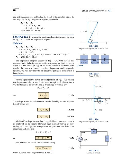
- Page 634 and 635: a c v � 24 sin qt ⇒ phasor form
- Page 636 and 637: a c v � 15 sin qt ⇒ phasor nota
- Page 640 and 641: a c In rectangular form, and VR �
- Page 642 and 643: a c Time domain: In the time domain
- Page 644 and 645: a c or E � V R � V L � V C wh
- Page 646 and 647: a c (6�0)*(50�30)/((6�0)�(9
- Page 648 and 649: a c Therefore, E � �(1�3�.3
- Page 650 and 651: a c f � 1 kHz XC � � �15.92
- Page 652 and 653: a c f � 0 Hz XC � � ⇒ very
- Page 654 and 655: a c ohms and the short-circuit equi
- Page 656 and 657: a c elements by 90°, and leads the
- Page 658 and 659: a c EXAMPLE 15.12 For the network o
- Page 660 and 661: a c EXAMPLE 15.14 Find the admittan
- Page 662 and 663: a c I Admittance diagram: As shown
- Page 664 and 665: a c E Admittance diagram: As shown
- Page 666 and 667: a c Phasor notation: As shown in Fi
- Page 668 and 669: a c Using Eq. (15.32), we obtain G
- Page 670 and 671: a c on the total impedance at that
- Page 672 and 673: a c 90° 60° 45° 30° 0° θ T In
- Page 674 and 675: a c 0° -30° -45° -60° -90° θL
- Page 676 and 677: a c The total impedance at the freq
- Page 678 and 679: a c Solution: Rp � 8k� Xp (resu
- Page 680 and 681: a c I = 12 A ∠ 0° FIG. 15.95 Ser
- Page 682 and 683: a c + e - a + v R - R impedance. Th
- Page 684 and 685: a c Switched outlets Parallel outle
- Page 686 and 687: a c transfer of power (see Section
- Page 688 and 689:
a c Consequently, the sound generat
- Page 690 and 691:
a c V applied 170 80.24 V(volts) V
- Page 692 and 693:
a c Run PSpice key. The result will
- Page 694 and 695:
a c Electronics Workbench We will n
- Page 696 and 697:
a c PROBLEMS SECTION 15.2 Impedance
- Page 698 and 699:
a c 7. For the circuit of Fig. 15.1
- Page 700 and 701:
a c + E = 20 V ∠ 70° - 20 � (a
- Page 702 and 703:
a c SECTION 15.7 Admittance and Sus
- Page 704 and 705:
a c 31. Repeat Problem 30 for the c
- Page 706 and 707:
a c 41. For the network of Fig. 15.
- Page 708:
a c GLOSSARY Admittance A measure o
- Page 711 and 712:
710 ⏐⏐⏐ SERIES-PARALLEL ac NE
- Page 713 and 714:
712 ⏐⏐⏐ SERIES-PARALLEL ac NE
- Page 715 and 716:
714 ⏐⏐⏐ SERIES-PARALLEL ac NE
- Page 717 and 718:
716 ⏐⏐⏐ SERIES-PARALLEL ac NE
- Page 719 and 720:
718 ⏐⏐⏐ SERIES-PARALLEL ac NE
- Page 721 and 722:
720 ⏐⏐⏐ SERIES-PARALLEL ac NE
- Page 723 and 724:
722 ⏐⏐⏐ SERIES-PARALLEL ac NE
- Page 725 and 726:
724 ⏐⏐⏐ SERIES-PARALLEL ac NE
- Page 727 and 728:
726 ⏐⏐⏐ SERIES-PARALLEL ac NE
- Page 729 and 730:
728 ⏐⏐⏐ SERIES-PARALLEL ac NE
- Page 731 and 732:
730 ⏐⏐⏐ SERIES-PARALLEL ac NE
- Page 733 and 734:
732 ⏐⏐⏐ SERIES-PARALLEL ac NE
- Page 735 and 736:
734 ⏐⏐⏐ SERIES-PARALLEL ac NE
- Page 737 and 738:
736 ⏐⏐⏐ SERIES-PARALLEL ac NE
- Page 739 and 740:
738 ⏐⏐⏐ SERIES-PARALLEL ac NE
- Page 741 and 742:
740 ⏐⏐⏐ SERIES-PARALLEL ac NE
- Page 743 and 744:
742 ⏐⏐⏐ SERIES-PARALLEL ac NE
- Page 745 and 746:
744 ⏐⏐⏐ METHODS OF ANALYSIS A
- Page 747 and 748:
746 ⏐⏐⏐ METHODS OF ANALYSIS A
- Page 749 and 750:
748 ⏐⏐⏐ METHODS OF ANALYSIS A
- Page 751 and 752:
750 ⏐⏐⏐ METHODS OF ANALYSIS A
- Page 753 and 754:
752 ⏐⏐⏐ METHODS OF ANALYSIS A
- Page 755 and 756:
754 ⏐⏐⏐ METHODS OF ANALYSIS A
- Page 757 and 758:
756 ⏐⏐⏐ METHODS OF ANALYSIS A
- Page 759 and 760:
758 ⏐⏐⏐ METHODS OF ANALYSIS A
- Page 761 and 762:
760 ⏐⏐⏐ METHODS OF ANALYSIS A
- Page 763 and 764:
762 ⏐⏐⏐ METHODS OF ANALYSIS A
- Page 765 and 766:
764 ⏐⏐⏐ METHODS OF ANALYSIS A
- Page 767 and 768:
766 ⏐⏐⏐ METHODS OF ANALYSIS A
- Page 769 and 770:
768 ⏐⏐⏐ METHODS OF ANALYSIS A
- Page 771 and 772:
770 ⏐⏐⏐ METHODS OF ANALYSIS A
- Page 773 and 774:
772 ⏐⏐⏐ METHODS OF ANALYSIS A
- Page 775 and 776:
774 ⏐⏐⏐ METHODS OF ANALYSIS A
- Page 777 and 778:
776 ⏐⏐⏐ METHODS OF ANALYSIS A
- Page 779 and 780:
778 ⏐⏐⏐ METHODS OF ANALYSIS A
- Page 781 and 782:
780 ⏐⏐⏐ METHODS OF ANALYSIS A
- Page 783 and 784:
782 ⏐⏐⏐ METHODS OF ANALYSIS A
- Page 785 and 786:
784 ⏐⏐⏐ METHODS OF ANALYSIS A
- Page 787 and 788:
786 ⏐⏐⏐ METHODS OF ANALYSIS A
- Page 789 and 790:
788 ⏐⏐⏐ METHODS OF ANALYSIS A
- Page 792 and 793:
18 Network Theorems (ac) 18.1 INTRO
- Page 794 and 795:
Th Z 1 E 1- + Z 1 I s1 j 4 � Z1
- Page 796 and 797:
Th EXAMPLE 18.4 For the network of
- Page 798 and 799:
Th pendent sources. The solution ob
- Page 800 and 801:
Th is the replacement of the term r
- Page 802 and 803:
Th Z1 � R1 � j XL1 � 6 ��
- Page 804 and 805:
Th will behave like the actual tran
- Page 806 and 807:
Th obtained by applying a source of
- Page 808 and 809:
Th Method 3: See Fig. 18.49. Eg Ig
- Page 810 and 811:
Th or Eoc�1 � � � k1k2R2
- Page 812 and 813:
Th Independent Sources The procedur
- Page 814 and 815:
Th Solution: Steps 1 and 2 (Fig. 18
- Page 816 and 817:
Th The Norton equivalent circuit ap
- Page 818 and 819:
Th so Eg(1 � h) � Ig[R1 � (1
- Page 820 and 821:
Th + E = 9 V ∠ 0° - Z1Z 2 (10
- Page 822 and 823:
Th (8.54 V) 72.93 and Pmax � �
- Page 824 and 825:
Th ��� ��� ����
- Page 826 and 827:
Th For 100 W, Is � � Np �Ip
- Page 828 and 829:
Th Redrawing the network as shown i
- Page 830 and 831:
Th 0.5 -0.5 v s (volts) 0 T /2 T -T
- Page 832 and 833:
Th culation of �32.74° of Exampl
- Page 834 and 835:
Th FIG. 18.101 Using PSpice to dete
- Page 836 and 837:
Th FIG. 18.104 The output file for
- Page 838 and 839:
Th FIG. 18.107 Using PSpice to dete
- Page 840 and 841:
Th *5. Using superposition, find th
- Page 842 and 843:
Th PROBLEMS ⏐⏐⏐ 841 11. Find
- Page 844 and 845:
Th PROBLEMS ⏐⏐⏐ 843 20. Find
- Page 846 and 847:
Th PROBLEMS ⏐⏐⏐ 845 *40. Find
- Page 848 and 849:
Th GLOSSARY ⏐⏐⏐ 847 49. Using
- Page 850 and 851:
19 Power (ac) 19.1 INTRODUCTION The
- Page 852 and 853:
P q s Power delivered to element by
- Page 854 and 855:
P q s The reason for rating some el
- Page 856 and 857:
P q s If the average power is zero,
- Page 858 and 859:
P q s 2 V and QC � �� (VAR) (
- Page 860 and 861:
P q s j I 2 X L = Q L I 2 X C = Q C
- Page 862 and 863:
P q s Thus, PT 600 W Fp ���
- Page 864 and 865:
P q s Motor: h � Pi � � �45
- Page 866 and 867:
P q s + E = E ∠0° - I L Solving
- Page 868 and 869:
P q s The equivalent parallel load
- Page 870 and 871:
P q s As the name implies, power-fa
- Page 872 and 873:
P q s duced, the eddy current loss
- Page 874 and 875:
P q s The vast majority of generato
- Page 876 and 877:
P q s 349.2 kW � 240 kW � 109.2
- Page 878 and 879:
P q s Peak icon to the right of the
- Page 880 and 881:
P q s small region below the axis i
- Page 882 and 883:
P q s 6. For the circuit of Fig. 19
- Page 884 and 885:
P q s *14. For the circuit of Fig.
- Page 886:
P q s SECTION 19.10 Effective Resis
- Page 889 and 890:
888 ⏐⏐⏐ RESONANCE E s + - Sou
- Page 891 and 892:
890 ⏐⏐⏐ RESONANCE Q L = I 2 X
- Page 893 and 894:
892 ⏐⏐⏐ RESONANCE R R( f ) 0
- Page 895 and 896:
894 ⏐⏐⏐ RESONANCE f < f s: ne
- Page 897 and 898:
896 ⏐⏐⏐ RESONANCE Solving the
- Page 899 and 900:
898 ⏐⏐⏐ RESONANCE As Q s of t
- Page 901 and 902:
900 ⏐⏐⏐ RESONANCE b. Since Qs
- Page 903 and 904:
902 ⏐⏐⏐ RESONANCE I Z T Y T R
- Page 905 and 906:
904 ⏐⏐⏐ RESONANCE R l Z Tm Z
- Page 907 and 908:
906 ⏐⏐⏐ RESONANCE Setting the
- Page 909 and 910:
908 ⏐⏐⏐ RESONANCE Inductive R
- Page 911 and 912:
910 ⏐⏐⏐ RESONANCE For an idea
- Page 913 and 914:
912 ⏐⏐⏐ RESONANCE TABLE 20.1
- Page 915 and 916:
914 ⏐⏐⏐ RESONANCE Example 20.
- Page 917 and 918:
916 ⏐⏐⏐ RESONANCE I e. Ql ≥
- Page 919 and 920:
918 ⏐⏐⏐ RESONANCE Therefore,
- Page 921 and 922:
920 ⏐⏐⏐ RESONANCE Volume Full
- Page 923 and 924:
922 ⏐⏐⏐ RESONANCE bandwidth
- Page 925 and 926:
924 ⏐⏐⏐ RESONANCE FIG. 20.43
- Page 927 and 928:
926 ⏐⏐⏐ RESONANCE cursor esta
- Page 929 and 930:
928 ⏐⏐⏐ RESONANCE FIG. 20.48
- Page 931 and 932:
930 ⏐⏐⏐ RESONANCE I 2 mA IL I
- Page 933 and 934:
932 ⏐⏐⏐ RESONANCE ZT I = 5 mA
- Page 935 and 936:
934 ⏐⏐⏐ RESONANCE Z Tp GLOSSA
- Page 937 and 938:
936 ⏐⏐⏐ TRANSFORMERS + e p -
- Page 939 and 940:
938 ⏐⏐⏐ TRANSFORMERS L p = 20
- Page 941 and 942:
940 ⏐⏐⏐ TRANSFORMERS revealin
- Page 943 and 944:
942 ⏐⏐⏐ TRANSFORMERS Since th
- Page 945 and 946:
944 ⏐⏐⏐ TRANSFORMERS Solution
- Page 947 and 948:
946 ⏐⏐⏐ TRANSFORMERS Public a
- Page 949 and 950:
948 ⏐⏐⏐ TRANSFORMERS + v x -
- Page 951 and 952:
950 ⏐⏐⏐ TRANSFORMERS + V g -
- Page 953 and 954:
952 ⏐⏐⏐ TRANSFORMERS + V g -
- Page 955 and 956:
954 ⏐⏐⏐ TRANSFORMERS (a) (b)
- Page 957 and 958:
956 ⏐⏐⏐ TRANSFORMERS polariti
- Page 959 and 960:
958 ⏐⏐⏐ TRANSFORMERS Iron cor
- Page 961 and 962:
960 ⏐⏐⏐ TRANSFORMERS Primary
- Page 963 and 964:
962 ⏐⏐⏐ TRANSFORMERS Z i + E
- Page 965 and 966:
964 ⏐⏐⏐ TRANSFORMERS Source +
- Page 967 and 968:
966 ⏐⏐⏐ TRANSFORMERS ��
- Page 969 and 970:
968 ⏐⏐⏐ TRANSFORMERS insertio
- Page 971 and 972:
970 ⏐⏐⏐ TRANSFORMERS FIG. 21.
- Page 973 and 974:
972 ⏐⏐⏐ TRANSFORMERS + Vg = 2
- Page 975 and 976:
974 ⏐⏐⏐ TRANSFORMERS q = 1000
- Page 978 and 979:
22 Polyphase Systems 22.1 INTRODUCT
- Page 980 and 981:
0.866 E m(CN) 0.866 E m(BN) This is
- Page 982 and 983:
E BC The length x is C B + - E CN E
- Page 984 and 985:
B C E BC E CA (a) ⎪ ⎬ ⎪ ⎭ E
- Page 986 and 987:
. EL � �3�Ef � (1.73)(120 V
- Page 988 and 989:
E CA = 150 V ∠ v 3 b. Vf � EL.T
- Page 990 and 991:
I Bb I AC 30° 120° It can be show
- Page 992 and 993:
The phase voltages are Van � IanZ
- Page 994 and 995:
Power Factor The power factor of th
- Page 996 and 997:
Power Factor S T � 3S f � �3
- Page 998 and 999:
A + EAN - or EAN � IfZline � Vf
- Page 1000 and 1001:
methods of determining whether the
- Page 1002 and 1003:
IBb � Ibc � Iab � 8.32 A �
- Page 1004 and 1005:
or multiphase, result in a total lo
- Page 1006 and 1007:
40,000 V �120° � 33,200 V �
- Page 1008 and 1009:
7. For the system of Fig. 22.39, fi
- Page 1010 and 1011:
C 14. Repeat Problem 13 if the phas
- Page 1012 and 1013:
3-phase ∆-connected generator Pha
- Page 1014 and 1015:
*43. The Y-Y system of Fig. 22.48 h
- Page 1016:
GLOSSARY �-connected ac generator
- Page 1019 and 1020:
1018 ⏐⏐⏐ DECIBELS, FILTERS, A
- Page 1021 and 1022:
1020 ⏐⏐⏐ DECIBELS, FILTERS, A
- Page 1023 and 1024:
1022 ⏐⏐⏐ DECIBELS, FILTERS, A
- Page 1025 and 1026:
1024 ⏐⏐⏐ DECIBELS, FILTERS, A
- Page 1027 and 1028:
1026 ⏐⏐⏐ DECIBELS, FILTERS, A
- Page 1029 and 1030:
1028 ⏐⏐⏐ DECIBELS, FILTERS, A
- Page 1031 and 1032:
1030 ⏐⏐⏐ DECIBELS, FILTERS, A
- Page 1033 and 1034:
1032 ⏐⏐⏐ DECIBELS, FILTERS, A
- Page 1035 and 1036:
1034 ⏐⏐⏐ DECIBELS, FILTERS, A
- Page 1037 and 1038:
1036 ⏐⏐⏐ DECIBELS, FILTERS, A
- Page 1039 and 1040:
1038 ⏐⏐⏐ DECIBELS, FILTERS, A
- Page 1041 and 1042:
1040 ⏐⏐⏐ DECIBELS, FILTERS, A
- Page 1043 and 1044:
1042 ⏐⏐⏐ DECIBELS, FILTERS, A
- Page 1045 and 1046:
1044 ⏐⏐⏐ DECIBELS, FILTERS, A
- Page 1047 and 1048:
1046 ⏐⏐⏐ DECIBELS, FILTERS, A
- Page 1049 and 1050:
1048 ⏐⏐⏐ DECIBELS, FILTERS, A
- Page 1051 and 1052:
1050 ⏐⏐⏐ DECIBELS, FILTERS, A
- Page 1053 and 1054:
1052 ⏐⏐⏐ DECIBELS, FILTERS, A
- Page 1055 and 1056:
1054 ⏐⏐⏐ DECIBELS, FILTERS, A
- Page 1057 and 1058:
1056 ⏐⏐⏐ DECIBELS, FILTERS, A
- Page 1059 and 1060:
1058 ⏐⏐⏐ DECIBELS, FILTERS, A
- Page 1061 and 1062:
1060 ⏐⏐⏐ DECIBELS, FILTERS, A
- Page 1063 and 1064:
1062 ⏐⏐⏐ DECIBELS, FILTERS, A
- Page 1065 and 1066:
1064 ⏐⏐⏐ DECIBELS, FILTERS, A
- Page 1067 and 1068:
1066 ⏐⏐⏐ DECIBELS, FILTERS, A
- Page 1069 and 1070:
1068 ⏐⏐⏐ DECIBELS, FILTERS, A
- Page 1071 and 1072:
1070 ⏐⏐⏐ DECIBELS, FILTERS, A
- Page 1073 and 1074:
1072 ⏐⏐⏐ DECIBELS, FILTERS, A
- Page 1075 and 1076:
1074 ⏐⏐⏐ DECIBELS, FILTERS, A
- Page 1077 and 1078:
1076 ⏐⏐⏐ DECIBELS, FILTERS, A
- Page 1079 and 1080:
1078 ⏐⏐⏐ DECIBELS, FILTERS, A
- Page 1081 and 1082:
1080 ⏐⏐⏐ DECIBELS, FILTERS, A
- Page 1083 and 1084:
1082 ⏐⏐⏐ DECIBELS, FILTERS, A
- Page 1085 and 1086:
1084 ⏐⏐⏐ DECIBELS, FILTERS, A
- Page 1087 and 1088:
1086 ⏐⏐⏐ DECIBELS, FILTERS, A
- Page 1089 and 1090:
1088 ⏐⏐⏐ DECIBELS, FILTERS, A
- Page 1091 and 1092:
1090 ⏐⏐⏐ DECIBELS, FILTERS, A
- Page 1093 and 1094:
1092 ⏐⏐⏐ DECIBELS, FILTERS, A
- Page 1095 and 1096:
1094 ⏐⏐⏐ PULSE WAVEFORMS AND
- Page 1097 and 1098:
1096 ⏐⏐⏐ PULSE WAVEFORMS AND
- Page 1099 and 1100:
1098 ⏐⏐⏐ PULSE WAVEFORMS AND
- Page 1101 and 1102:
1100 ⏐⏐⏐ PULSE WAVEFORMS AND
- Page 1103 and 1104:
1102 ⏐⏐⏐ PULSE WAVEFORMS AND
- Page 1105 and 1106:
1104 ⏐⏐⏐ PULSE WAVEFORMS AND
- Page 1107 and 1108:
1106 ⏐⏐⏐ PULSE WAVEFORMS AND
- Page 1109 and 1110:
1108 ⏐⏐⏐ PULSE WAVEFORMS AND
- Page 1111 and 1112:
1110 ⏐⏐⏐ PULSE WAVEFORMS AND
- Page 1113 and 1114:
1112 ⏐⏐⏐ PULSE WAVEFORMS AND
- Page 1115 and 1116:
1114 ⏐⏐⏐ PULSE WAVEFORMS AND
- Page 1117 and 1118:
1116 ⏐⏐⏐ PULSE WAVEFORMS AND
- Page 1119 and 1120:
1118 ⏐⏐⏐ PULSE WAVEFORMS AND
- Page 1121 and 1122:
1120 ⏐⏐⏐ PULSE WAVEFORMS AND
- Page 1124 and 1125:
25 Nonsinusoidal Circuits 25.1 INTR
- Page 1126 and 1127:
NON Average Value: A 0 The dc term
- Page 1128 and 1129:
NON f(t) � �f � t � � T 2
- Page 1130 and 1131:
NON EXAMPLE 25.1 Determine which co
- Page 1132 and 1133:
NON 1 sin qt i t 1 (i = 0) FIG. 25.
- Page 1134 and 1135:
NON Vm 0 v 1 (a) and v � Vm�1
- Page 1136 and 1137:
NON v(a) � V 0 � V m1 sin a �
- Page 1138 and 1139:
NON EXAMPLE 25.7 The input to the c
- Page 1140 and 1141:
NON ZT1 � 6 ��j 37.7 ��38
- Page 1142 and 1143:
NON FIG. 25.28 Using PSpice to appl
- Page 1144 and 1145:
NON you can change the range to 0 H
- Page 1146 and 1147:
NON 9. Find the total average power
- Page 1148:
NON 24. Given any nonsinusoidal fun
- Page 1151 and 1152:
1150 ⏐⏐⏐ SYSTEM ANALYSIS: AN
- Page 1153 and 1154:
1152 ⏐⏐⏐ SYSTEM ANALYSIS: AN
- Page 1155 and 1156:
1154 ⏐⏐⏐ SYSTEM ANALYSIS: AN
- Page 1157 and 1158:
1156 ⏐⏐⏐ SYSTEM ANALYSIS: AN
- Page 1159 and 1160:
1158 ⏐⏐⏐ SYSTEM ANALYSIS: AN
- Page 1161 and 1162:
1160 ⏐⏐⏐ SYSTEM ANALYSIS: AN
- Page 1163 and 1164:
1162 ⏐⏐⏐ SYSTEM ANALYSIS: AN
- Page 1165 and 1166:
1164 ⏐⏐⏐ SYSTEM ANALYSIS: AN
- Page 1167 and 1168:
1166 ⏐⏐⏐ SYSTEM ANALYSIS: AN
- Page 1169 and 1170:
1168 ⏐⏐⏐ SYSTEM ANALYSIS: AN
- Page 1171 and 1172:
1170 ⏐⏐⏐ SYSTEM ANALYSIS: AN
- Page 1173 and 1174:
1172 ⏐⏐⏐ SYSTEM ANALYSIS: AN
- Page 1175 and 1176:
1174 ⏐⏐⏐ SYSTEM ANALYSIS: AN
- Page 1177 and 1178:
1176 ⏐⏐⏐ SYSTEM ANALYSIS: AN
- Page 1179 and 1180:
1178 ⏐⏐⏐ SYSTEM ANALYSIS: AN
- Page 1181 and 1182:
1180 ⏐⏐⏐ SYSTEM ANALYSIS: AN
- Page 1183 and 1184:
1182 ⏐⏐⏐ SYSTEM ANALYSIS: AN
- Page 1185 and 1186:
1184 ⏐⏐⏐ SYSTEM ANALYSIS: AN
- Page 1187 and 1188:
1186 ⏐⏐⏐ SYSTEM ANALYSIS: AN
- Page 1189 and 1190:
1188 ⏐⏐⏐ SYSTEM ANALYSIS: AN
- Page 1191 and 1192:
1190 ⏐⏐⏐ SYSTEM ANALYSIS: AN
- Page 1193 and 1194:
1192 Appendixes APPENDIX A PSpice,
- Page 1195 and 1196:
1194 ⏐⏐⏐ APPENDIXES A.3 Mathc
- Page 1197 and 1198:
1196 ⏐⏐⏐ APPENDIXES To Conver
- Page 1199 and 1200:
1198 Appendix C DETERMINANTS Determ
- Page 1201 and 1202:
1200 ⏐⏐⏐ APPENDIXES 2 3 �3
- Page 1203 and 1204:
1202 ⏐⏐⏐ APPENDIXES x � War
- Page 1205 and 1206:
1204 ⏐⏐⏐ APPENDIXES D Note th
- Page 1207 and 1208:
1206 Appendix D COLOR CODING OF MOL
- Page 1209 and 1210:
1208 Appendix F MAGNETIC PARAMETER
- Page 1211 and 1212:
1210 ⏐⏐⏐ APPENDIXES and the p
- Page 1213 and 1214:
1212 ⏐⏐⏐ APPENDIXES 3. (a) 16
- Page 1215 and 1216:
1214 ⏐⏐⏐ APPENDIXES (b) 50(1
- Page 1217 and 1218:
1216 ⏐⏐⏐ APPENDIXES (f) 300 W
- Page 1219 and 1220:
1218 ⏐⏐⏐ APPENDIXES 9. (a) E