FR60 MB91460E Series - Microcontrollers - Fujitsu
FR60 MB91460E Series - Microcontrollers - Fujitsu
FR60 MB91460E Series - Microcontrollers - Fujitsu

You also want an ePaper? Increase the reach of your titles
YUMPU automatically turns print PDFs into web optimized ePapers that Google loves.
<strong>MB91460E</strong> <strong>Series</strong><br />
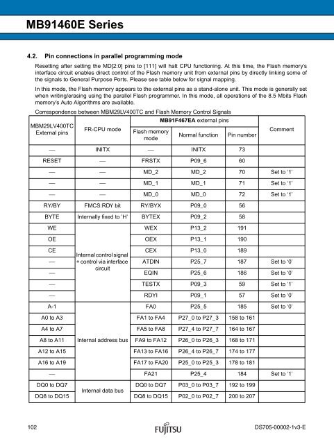
4.2. Pin connections in parallel programming mode<br />
Resetting after setting the MD[2:0] pins to [111] will halt CPU functioning. At this time, the Flash memory’s<br />
interface circuit enables direct control of the Flash memory unit from external pins by directly linking some of<br />
the signals to General Purpose Ports. Please see table below for signal mapping.<br />
In this mode, the Flash memory appears to the external pins as a stand-alone unit. This mode is generally set<br />
when writing/erasing using the parallel Flash programmer. In this mode, all operations of the 8.5 Mbits Flash<br />
memory’s Auto Algorithms are available.<br />
Correspondence between MBM29LV400TC and Flash Memory Control Signals<br />
MBM29LV400TC<br />
External pins<br />
FR-CPU mode<br />
Flash memory<br />
mode<br />
MB91F467EA external pins<br />
Normal function Pin number<br />
⎯ INITX ⎯ INITX 73<br />
RESET ⎯ FRSTX P09_6 60<br />
Comment<br />
⎯ ⎯ MD_2 MD_2 70 Set to ‘1’<br />
⎯ ⎯ MD_1 MD_1 71 Set to ‘1’<br />
⎯ ⎯ MD_0 MD_0 72 Set to ‘1’<br />
RY/BY FMCS:RDY bit RY/BYX P09_0 56<br />
BYTE Internally fixed to ’H’ BYTEX P09_2 58<br />
WE<br />
WEX P13_2 191<br />
OE OEX P13_1 190<br />
CE<br />
Internal control signal<br />
CEX P13_0 189<br />
⎯ + control via interface ATDIN P25_7 187 Set to ‘0’<br />
⎯<br />
circuit<br />
EQIN P25_6 186 Set to ‘0’<br />
⎯ TESTX P09_3 59 Set to ‘1’<br />
⎯ RDYI P09_1 57 Set to ‘0’<br />
A-1<br />
FA0 P25_5 185 Set to ‘0’<br />
A0 to A3 FA1 to FA4 P27_0 to P27_3 158 to 161<br />
A4 to A7 FA5 to FA8 P27_4 to P27_7 164 to 167<br />
A8 to A11 Internal address bus FA9 to FA12 P26_0 to P26_3 168 to 171<br />
A12 to A15 FA13 to FA16 P26_4 to P26_7 174 to 177<br />
A16 to A19 FA17 to FA20 P25_0 to P25_3 178 to 181<br />
⎯ FA21 P25_4 184 Set to ‘1’<br />
DQ0 to DQ7<br />
DQ0 to DQ7 P03_0 to P03_7 192 to 199<br />
Internal data bus<br />
DQ8 to DQ15 DQ8 to DQ15 P02_0 to P02_7 200 to 207<br />
102 DS705-00002-1v3-E