FR60 MB91460E Series - Microcontrollers - Fujitsu
FR60 MB91460E Series - Microcontrollers - Fujitsu
FR60 MB91460E Series - Microcontrollers - Fujitsu

Create successful ePaper yourself
Turn your PDF publications into a flip-book with our unique Google optimized e-Paper software.
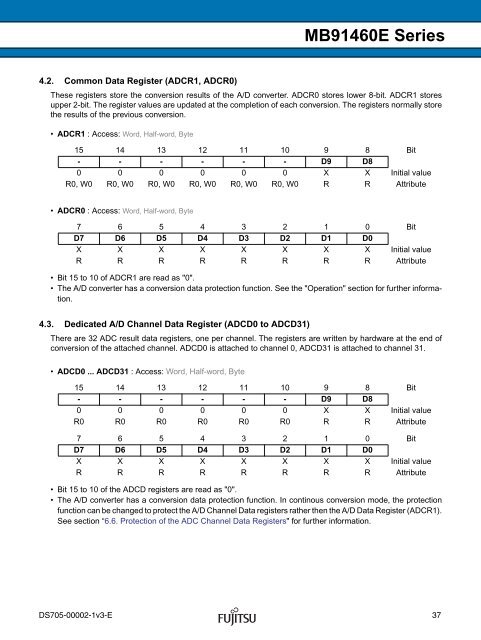
4.2. Common Data Register (ADCR1, ADCR0)<br />
<strong>MB91460E</strong> <strong>Series</strong><br />
These registers store the conversion results of the A/D converter. ADCR0 stores lower 8-bit. ADCR1 stores<br />
upper 2-bit. The register values are updated at the completion of each conversion. The registers normally store<br />
the results of the previous conversion.<br />
• ADCR1 : Access: Word, Half-word, Byte<br />
15 14 13 12 11 10 9 8 Bit<br />
- - - - - - D9 D8<br />
0 0 0 0 0 0 X X Initial value<br />
R0, W0 R0, W0 R0, W0 R0, W0 R0, W0 R0, W0 R R Attribute<br />
• ADCR0 : Access: Word, Half-word, Byte<br />
7 6 5 4 3 2 1 0 Bit<br />
D7 D6 D5 D4 D3 D2 D1 D0<br />
X X X X X X X X Initial value<br />
R R R R R R R R Attribute<br />
• Bit 15 to 10 of ADCR1 are read as "0".<br />
• The A/D converter has a conversion data protection function. See the "Operation" section for further information.<br />
4.3. Dedicated A/D Channel Data Register (ADCD0 to ADCD31)<br />
There are 32 ADC result data registers, one per channel. The registers are written by hardware at the end of<br />
conversion of the attached channel. ADCD0 is attached to channel 0, ADCD31 is attached to channel 31.<br />
• ADCD0 ... ADCD31 : Access: Word, Half-word, Byte<br />
15 14 13 12 11 10 9 8 Bit<br />
- - - - - - D9 D8<br />
0 0 0 0 0 0 X X Initial value<br />
R0 R0 R0 R0 R0 R0 R R Attribute<br />
7 6 5 4 3 2 1 0 Bit<br />
D7 D6 D5 D4 D3 D2 D1 D0<br />
X X X X X X X X Initial value<br />
R R R R R R R R Attribute<br />
• Bit 15 to 10 of the ADCD registers are read as "0".<br />
• The A/D converter has a conversion data protection function. In continous conversion mode, the protection<br />
function can be changed to protect the A/D Channel Data registers rather then the A/D Data Register (ADCR1).<br />
See section “6.6. Protection of the ADC Channel Data Registers" for further information.<br />
DS705-00002-1v3-E 37