FR60 MB91460E Series - Microcontrollers - Fujitsu
FR60 MB91460E Series - Microcontrollers - Fujitsu
FR60 MB91460E Series - Microcontrollers - Fujitsu

Create successful ePaper yourself
Turn your PDF publications into a flip-book with our unique Google optimized e-Paper software.
<strong>MB91460E</strong> <strong>Series</strong><br />
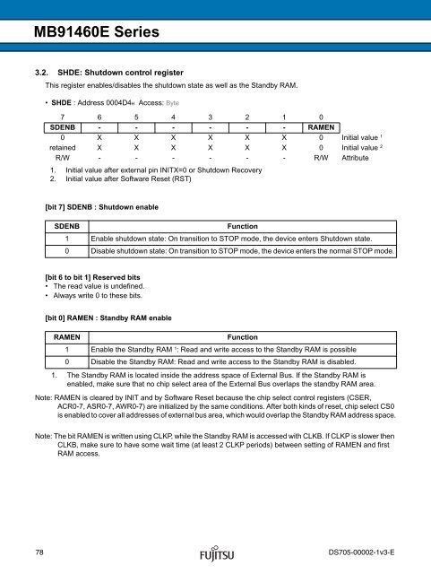
3.2. SHDE: Shutdown control register<br />
This register enables/disables the shutdown state as well as the Standby RAM.<br />
• SHDE : Address 0004D4H Access: Byte<br />
7 6 5 4 3 2 1 0<br />
SDENB - - - - - - RAMEN<br />
0 X X X X X X 0 Initial value 1<br />
retained X X X X X X 0 Initial value<br />
1. Initial value after external pin INITX=0 or Shutdown Recovery<br />
2<br />
R/W - - - - - - R/W Attribute<br />
2. Initial value after Software Reset (RST)<br />
[bit 7] SDENB : Shutdown enable<br />
SDENB Function<br />
1 Enable shutdown state: On transition to STOP mode, the device enters Shutdown state.<br />
0 Disable shutdown state: On transition to STOP mode, the device enters the normal STOP mode.<br />
[bit 6 to bit 1] Reserved bits<br />
• The read value is undefined.<br />
• Always write 0 to these bits.<br />
[bit 0] RAMEN : Standby RAM enable<br />
RAMEN Function<br />
1 Enable the Standby RAM 1 : Read and write access to the Standby RAM is possible<br />
0 Disable the Standby RAM: Read and write access to the Standby RAM is disabled.<br />
1. The Standby RAM is located inside the address space of External Bus. If the Standby RAM is<br />
enabled, make sure that no chip select area of the External Bus overlaps the standby RAM area.<br />
Note: RAMEN is cleared by INIT and by Software Reset because the chip select control registers (CSER,<br />
ACR0-7, ASR0-7, AWR0-7) are initialized by the same conditions. After both kinds of reset, chip select CS0<br />
is enabled to cover all addresses of external bus area, which would overlap the Standby RAM address space.<br />
Note: The bit RAMEN is written using CLKP, while the Standby RAM is accessed with CLKB. If CLKP is slower then<br />
CLKB, make sure to have some wait time (at least 2 CLKP periods) between setting of RAMEN and first<br />
RAM access.<br />
78 DS705-00002-1v3-E