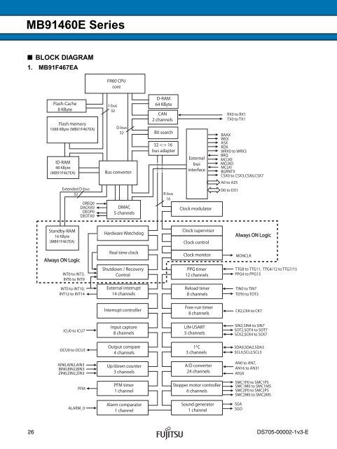
- Page 1 and 2: FUJITSU SEMICONDUCTOR DATA SHEET 32
- Page 3 and 4: MB91460E Series (Continued) • Rea
- Page 5 and 6: MB91460E Series Sound Generator 1 c
- Page 7 and 8: MB91460E Series DS705-00002-1v3-E 7
- Page 9 and 10: (Continued) Pin no. Pin name I/O 66
- Page 11 and 12: (Continued) Pin no. Pin name I/O 10
- Page 13 and 14: (Continued) Pin no. Pin name I/O 16
- Page 15 and 16: 2. Power supply/Ground pins MB91460
- Page 17 and 18: Type Circuit Remarks MB91460E Serie
- Page 19 and 20: Type Circuit Remarks G Mask ROM and
- Page 21 and 22: Type Circuit Remarks M CMOS level t
- Page 23 and 24: (Continued) Example of using opposi
- Page 25: ■ NOTES ON DEBUGGER 1. Execution
- Page 29 and 30: 3. Block Diagram of A/D Converter T
- Page 31 and 32: 1. On MB91F467E, ADC1 does not exis
- Page 33 and 34: • ADCS1 : Access: Half-word, Byte
- Page 35 and 36: MB91460E Series [bit 9] STRT (Start
- Page 37 and 38: 4.2. Common Data Register (ADCR1, A
- Page 39 and 40: 4.5. A/D Channel Setting Register (
- Page 41 and 42: 5.2. Range Comparator Registers The
- Page 43 and 44: 5.2.3. Inverted Range Selection reg
- Page 45 and 46: MB91460E Series The interrupt condi
- Page 47 and 48: 6. Operation of A/D Converter MB914
- Page 49 and 50: 6.5. Scan Conversion The following
- Page 51 and 52: MB91460E Series The automatic inter
- Page 53 and 54: ■ CLOCK SUPERVISOR (New Feature)
- Page 55 and 56: 2.1. Clock Supervisor Control Regis
- Page 57 and 58: 3. Block Diagram Clock Supervisor M
- Page 59 and 60: MB91460E Series Figure 0-4 Timing D
- Page 61 and 62: MB91460E Series Figure 0-6 Timing D
- Page 63 and 64: MB91460E Series Figure 0-8 Timing D
- Page 65 and 66: 4.3. Re-enabling the RC-oscillator
- Page 67 and 68: MB91460E Series Figure 0-11 Timing
- Page 69 and 70: Timing Diagram: Waking up from Sub
- Page 71 and 72: 4.9. RTC mode (STOP mode with Real
- Page 73 and 74: 4.11. Check if reset was asserted b
- Page 75 and 76: ■ MB91460E Series DS705-00002-1v3
- Page 77 and 78:
2. Standby RAM MB91460E Series MB91
- Page 79 and 80:
3.3. EXTE: Shutdown recovery extern
- Page 81 and 82:
[bit 1] RTCF: Real Time Clock recov
- Page 83 and 84:
3.6. EXTLV1/2: Shutdown recovery ex
- Page 85 and 86:
4.1.3. Shutdown with Real Time Cloc
- Page 87 and 88:
4.1.8. External Interrupts: Level o
- Page 89 and 90:
4.3. Determining the Reset Source a
- Page 91 and 92:
4.5. I/O Behaviour in Shutdown Duri
- Page 93 and 94:
3. Programming model 3.1. Basic pro
- Page 95 and 96:
4.3. CCR (Condition Code Register)
- Page 97 and 98:
■ EMBEDDED PROGRAM/DATA MEMORY (F
- Page 99 and 100:
3.2. Flash access timing settings i
- Page 101 and 102:
4. Parallel Flash programming mode
- Page 103 and 104:
5. Poweron Sequence in parallel pro
- Page 105 and 106:
6.3. Security Vector FSV2 MB91460E
- Page 107 and 108:
■ MEMORY MAPS 1. MB91F467EA 00000
- Page 109 and 110:
Address 000000H 000004H 000008H Reg
- Page 111 and 112:
(Continued) Address 0000A0H Registe
- Page 113 and 114:
(Continued) Address 000180H Reserve
- Page 115 and 116:
(Continued) Address 000200H 000204H
- Page 117 and 118:
(Continued) Address 000348H 00034CH
- Page 119 and 120:
(Continued) Address 00048CH 000490H
- Page 121 and 122:
(Continued) Address + 0 + 1 Registe
- Page 123 and 124:
Address 000704H 000708H 00070CH 000
- Page 125 and 126:
(Continued) Address 000D80H 000D84H
- Page 127 and 128:
(Continued) Address 000E80H 000E84H
- Page 129 and 130:
(Continued) Address 002000H to 006F
- Page 131 and 132:
(Continued) Address 00C080H 00C084H
- Page 133 and 134:
(Continued) Address 00C1A0H 00C1A4H
- Page 135 and 136:
Address 00F09CH 00F0A0H 00F0A4H 00F
- Page 137 and 138:
32bit read/write dat[31:0] dat[31:0
- Page 139 and 140:
(Continued) Interrupt Decimal Inter
- Page 141 and 142:
(Continued) Interrupt Decimal Inter
- Page 143 and 144:
■ RECOMMENDED SETTINGS 1. PLL and
- Page 145 and 146:
MB91460E Series (Continued) Modulat
- Page 147 and 148:
MB91460E Series (Continued) Modulat
- Page 149 and 150:
(Continued) Modulation Degree (k) R
- Page 151 and 152:
“H” level average output curren
- Page 153 and 154:
2. Recommended operating conditions
- Page 155 and 156:
3. DC characteristics MB91460E Seri
- Page 157 and 158:
Parameter Symbol Analog inputleakag
- Page 159 and 160:
MB91460E Series 4. A/D converter ch
- Page 161 and 162:
Digital output 3FFH 3FEH 3FDH 004H
- Page 163 and 164:
5. Alarm comparator characteristics
- Page 165 and 166:
7. AC characteristics 7.1. Clock ti
- Page 167 and 168:
7.3. LIN-USART Timings at VDD5 = 3.
- Page 169 and 170:
7.4. I 2 C AC Timings at VDD5 = 3.0
- Page 171 and 172:
7.5. Free-run timer clock Input pul
- Page 173 and 174:
MCLKO CSXn delayed CSXn ASX ADDRESS
- Page 175 and 176:
MCLKO MCLKI CSXn WRXn (as byte enab
- Page 177 and 178:
MB91460E Series 7.7.4. Synchronous
- Page 179 and 180:
MB91460E Series 7.7.6. Asynchronous
- Page 181 and 182:
7.7.8. RDY waitcycle insertion Para
- Page 183 and 184:
7.7.10. Clock relationships MB91460
- Page 185 and 186:
MCLKO DACKX DEOP delayed DACKX dela
- Page 187 and 188:
MCLKO CSXn delayed CSXn ASX ADDRESS
- Page 189 and 190:
MCLKO MCLKI CSXn WRXn (as byte enab
- Page 191 and 192:
MB91460E Series 7.8.4. Synchronous
- Page 193 and 194:
MB91460E Series 7.8.6. Asynchronous
- Page 195 and 196:
7.8.8. RDY waitcycle insertion Para
- Page 197 and 198:
7.8.10. Clock relationships MCLKO
- Page 199 and 200:
MCLKO DACKX DEOP delayed DACKX dela
- Page 201 and 202:
■ PACKAGE DIMENSION 208-pin plast
- Page 203 and 204:
Version/ Date Ver. 0.8 2009-10-19 V
- Page 205 and 206:
■ CHANGES IN THIS EDITION DS705-0
- Page 207 and 208:
MEMO MB91460E Series DS705-00002-1v
- Page 209:
MB91460E Series DS705-00002-1v3-E 2