Edwin Jan Klein - Universiteit Twente
Edwin Jan Klein - Universiteit Twente
Edwin Jan Klein - Universiteit Twente

You also want an ePaper? Increase the reach of your titles
YUMPU automatically turns print PDFs into web optimized ePapers that Google loves.
Chapter 5<br />
5.1 Introduction<br />
The material system in which most of the resonators presented in this thesis have been<br />
fabricated is the silicon nitride/silicon oxide system (Si3N4/SiO2) [130]. The silicon<br />
nitride is used to fabricate the core of the waveguides while silicon oxide (e.g.<br />
thermal, TEOS or PECVD) is used in both the substrate and cladding layers. Both<br />
materials are highly compatible with CMOS technologies and can therefore benefit<br />
from all the advances made in these technologies.<br />
Silicon nitride was chosen due to its high refractive index of ≈1.98 at 1550 nm which,<br />
combined with silicon oxide as substrate or cladding layer, allows for potentially very<br />
small resonators, down to a radius of approximately 15 µm. In addition, the material<br />
is optically transparent from 400 nm to 2 um which makes it suitable for a wide range<br />
of applications and allows for low-loss high index waveguides with reported losses<br />
lower than 0.1 dB/cm [131]. Silicon nitride can be deposited in multiple layers of<br />
which the thickness can be controlled to within a few nanometers. Also, because the<br />
silicon nitride precursor gasses can be chosen to react to form stoichiometric Si3N4,<br />
the process is very stable concerning the refractive index. This opposed to for instance<br />
the SiliconOxiNitride process (SiON) where the ratios of the various precursors need<br />
to be carefully controlled during layer deposition to obtain a uniform refractive index,<br />
and from deposition to deposition for reproducibility. The use of silicon nitride,<br />
however, does place a constraint on the thickness of the silicon nitride layer. Due to<br />
tensile stress within the material it will crack and become unusable. The maximum<br />
safe deposition thickness of a silicon nitride layer is therefore no more than ≈340 nm.<br />
This thickness, however, allows for resonators as small as 15 µm which is more than<br />
sufficient for many applications.<br />
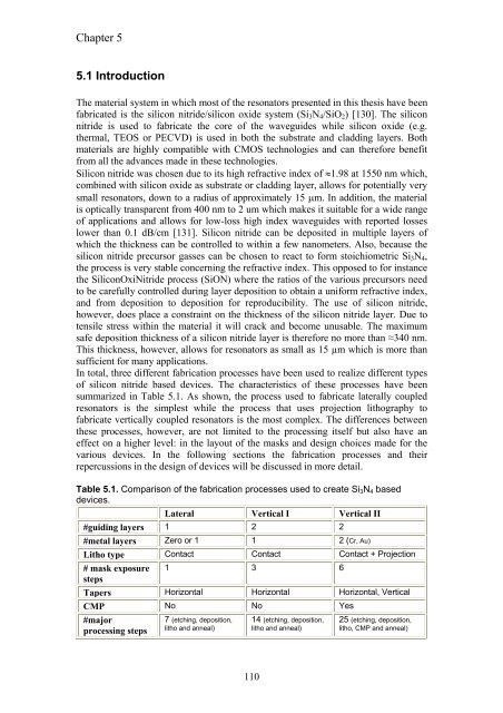
In total, three different fabrication processes have been used to realize different types<br />
of silicon nitride based devices. The characteristics of these processes have been<br />
summarized in Table 5.1. As shown, the process used to fabricate laterally coupled<br />
resonators is the simplest while the process that uses projection lithography to<br />
fabricate vertically coupled resonators is the most complex. The differences between<br />
these processes, however, are not limited to the processing itself but also have an<br />
effect on a higher level: in the layout of the masks and design choices made for the<br />
various devices. In the following sections the fabrication processes and their<br />
repercussions in the design of devices will be discussed in more detail.<br />
Table 5.1. Comparison of the fabrication processes used to create Si3N4 based<br />
devices.<br />
Lateral Vertical I Vertical II<br />
#guiding layers 1 2 2<br />
#metal layers Zero or 1 1 2 (Cr, Au)<br />
Litho type Contact Contact Contact + Projection<br />
# mask exposure<br />
steps<br />
1 3 6<br />
Tapers Horizontal Horizontal Horizontal, Vertical<br />
CMP No No Yes<br />
#major<br />
processing steps<br />
7 (etching, deposition,<br />
litho and anneal)<br />
14 (etching, deposition,<br />
litho and anneal)<br />
25 (etching, deposition,<br />
litho, CMP and anneal)<br />
110