Edwin Jan Klein - Universiteit Twente
Edwin Jan Klein - Universiteit Twente
Edwin Jan Klein - Universiteit Twente

You also want an ePaper? Increase the reach of your titles
YUMPU automatically turns print PDFs into web optimized ePapers that Google loves.
119<br />
Fabrication<br />
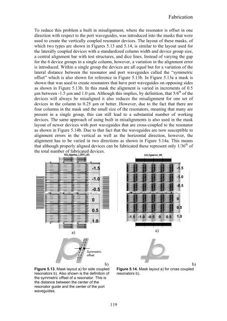
To reduce this problem a built in misalignment, where the resonator is offset in one<br />
direction with respect to the port waveguides, was introduced into the masks that were<br />
used to create the vertically coupled resonator devices. The layout of these masks, of<br />
which two types are shown in Figures 5.13 and 5.14, is similar to the layout used for<br />
the laterally coupled devices with a standardized column width and device group size,<br />
a central alignment bar with test structures, and dice lines. Instead of varying the gap<br />
for the 6 device groups in a single column, however, a variation in the alignment error<br />
is introduced. Within a single group the devices are all equal but for a variation of the<br />
lateral distance between the resonator and port waveguides called the “symmetric<br />
offset” which is also shown for reference in Figure 5.13b. In Figure 5.13a a mask is<br />
shown that was used to create resonators that have port waveguides on opposing sides<br />
as shown in Figure 5.13b. In this mask the alignment is varied in increments of 0.5<br />
µm between -1.5 µm and 1.0 µm. Although this implies, by definition, that 5/6 th of the<br />
devices will always be misaligned it also reduces the misalignment for one set of<br />
devices in the column to 0.25 µm or better. However, due to the fact that there are<br />
four columns in the mask and the small size of the resonators, meaning that many are<br />
present in a single group, this can still lead to a substantial number of working<br />
devices. The same approach of using built in misalignments is also used in the mask<br />
layout of newer devices with port waveguides that are cross-coupled to the resonator<br />
as shown in Figure 5.14b. Due to that fact that the waveguides are now susceptible to<br />
alignment errors in the vertical as well as the horizontal direction, however, the<br />
alignment has to be varied in two directions as shown in Figure 5.14a. This means<br />
that although properly aligned devices can be fabricated these represent only 1/36 th of<br />
the total number of fabricated devices.<br />
a)<br />
-1.5<br />
-1.0<br />
-0.5<br />
Symmetric<br />
offset<br />
Figure 5.13. Mask layout a) for side coupled<br />
resonators b). Also shown is the definition of<br />
the symmetric offset of a resonator. This is<br />
the distance between the center of the<br />
resonator guide and the center of the port<br />
waveguides.<br />
0<br />
0.5<br />
1.0<br />
-1.5 -1.0 -0.5 0 0.5<br />
b) b)<br />
Figure 5.14. Mask layout a) for cross coupled<br />
resonators b).<br />
a)<br />
-1.5<br />
-1.0<br />
-0.5<br />
0<br />
0.5<br />
1.0