Edwin Jan Klein - Universiteit Twente
Edwin Jan Klein - Universiteit Twente
Edwin Jan Klein - Universiteit Twente

You also want an ePaper? Increase the reach of your titles
YUMPU automatically turns print PDFs into web optimized ePapers that Google loves.
Chapter 7<br />
matrix is 300 µm and the horizontal distance is 250 µm. These distances were<br />
required to be able to fit the wiring of all the electrodes. Also, having some distance<br />
between the resonators will reduce the thermal crosstalk between the resonators. Also<br />
indicated in the figure are the horizontal taper sections and the electrode bonding<br />
pads. From the bond pads gold on chromium wires extend to the chromium heaters on<br />
top of the resonators in the router matrix. Because many of the resonators in the<br />
matrix interact with each other it can be difficult to interpret initial measurement<br />
results. Additional test waveguides were therefore incorporated in the design to help<br />
determine the resonance frequencies of the individual micro-resonators in each<br />
column.<br />
7.3.3 Improved OADM design<br />
The router design was to be fabricated in the new “Vertical II” fabrication process that<br />
used stepper lithography for the alignment and exposure of the resonator and port<br />
waveguides. Since not all of the image space on the reticle had been used for the<br />
router design the rest of the available image space was not only filled with several test<br />
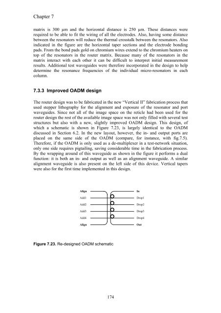
structures but also with a new, slightly improved OADM design. This design, of<br />
which a schematic is shown in Figure 7.23, is largely identical to the OADM<br />
discussed in Section 6.2. In the new layout, however, the in- and output ports are<br />
placed on the same side of the OADM (compare, for instance, with fig.7.5).<br />
Therefore, if the OADM is only used as a de-multiplexer in a test-network situation,<br />
only one side requires pigtailing, saving considerable time in the fabrication process.<br />
By the wrapping around of this waveguide as shown in the figure it performs a dual<br />
function: it is both an in- and output as well as an alignment waveguide. A similar<br />
alignment waveguide is also present on the left side of this device. Vertical tapers<br />
were also for the first time implemented in this design.<br />
Align<br />
Add1<br />
Add2<br />
Add3<br />
Add4<br />
Align<br />
Figure 7.23. Re-designed OADM schematic<br />
174<br />
In<br />
Drop1<br />
Drop2<br />
Drop3<br />
Drop4<br />
Out