Edwin Jan Klein - Universiteit Twente
Edwin Jan Klein - Universiteit Twente
Edwin Jan Klein - Universiteit Twente

You also want an ePaper? Increase the reach of your titles
YUMPU automatically turns print PDFs into web optimized ePapers that Google loves.
121<br />
Fabrication<br />
280 nm and an alignment accuracy better than 40 nm. The problems related to the<br />
accurate positioning of the resonator with respect to the waveguides are therefore<br />
essentially removed. The downside of using a stepper however lies in the maximum<br />
mask area that can be exposed. To achieve the high optical resolution the wafer<br />
stepper reduces the image(s) present on the reticle linearly by a factor of five. Due to<br />
this reduction and the image space available on the reticle the maximum area that can<br />
be exposed on the wafer is 22 x 27.4 mm for this specific stepper tool. This, however,<br />
is the maximum area that can be exposed in a single exposure step and uses up all the<br />
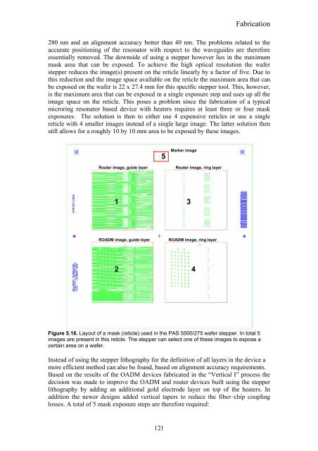
image space on the reticle. This poses a problem since the fabrication of a typical<br />
microring resonator based device with heaters requires at least three or four mask<br />
exposures. The solution is then to either use 4 expensive reticles or use a single<br />
reticle with 4 smaller images instead of a single large image. The latter solution then<br />
still allows for a roughly 10 by 10 mm area to be exposed by these images.<br />
Router image, guide layer Router image, ring layer<br />
1<br />
ROADM image, guide layer ROADM image, ring layer<br />
2<br />
Marker image<br />
Figure 5.16. Layout of a mask (reticle) used in the PAS 5500/275 wafer stepper. In total 5<br />
images are present in this reticle. The stepper can select one of these images to expose a<br />
certain area on a wafer.<br />
Instead of using the stepper lithography for the definition of all layers in the device a<br />
more efficient method can also be found, based on alignment accuracy requirements.<br />
Based on the results of the OADM devices fabricated in the “Vertical I” process the<br />
decision was made to improve the OADM and router devices built using the stepper<br />
lithography by adding an additional gold electrode layer on top of the heaters. In<br />
addition the newer designs added vertical tapers to reduce the fiber–chip coupling<br />
losses. A total of 5 mask exposure steps are therefore required:<br />
5<br />
3<br />
4