Edwin Jan Klein - Universiteit Twente
Edwin Jan Klein - Universiteit Twente
Edwin Jan Klein - Universiteit Twente

You also want an ePaper? Increase the reach of your titles
YUMPU automatically turns print PDFs into web optimized ePapers that Google loves.
Chapter 5<br />
wafer is used (step 1). The SiO2, with a thickness of 6-8 µm, serves as a buffer layer<br />
between the waveguides and the silicon substrate to prevent leakage of light into the<br />
substrate. On top of the SiO2 a 140-145 nm thick (varies slightly per application) layer<br />
of Si3N4 is deposited (step 2) using low-pressure chemical vapor deposition (LPCVD)<br />
at 800 °C. In this layer the waveguides are defined by first spinning a 1.5 µm thick<br />
layer of photoresist on top of the Si3N4 (step 3). After a pre-exposure bake of 1 minute<br />
at 95 °C this layer is exposed to UV light for 5.5 seconds through a chrome mask on a<br />
KARL SUSS MA 56M mask aligner (step 4). This mask, of which a small portion is<br />
shown in Figure 5.2 contains the definition of the waveguides, ring resonators, test<br />
structures and several supporting structures such as dice lines.<br />
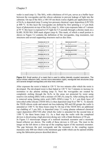
Figure 5.2. Small section of a mask that is used to define laterally coupled resonators. The<br />
layout shows reflectors (left), normal micro-resonators (right), waveguide test structures (loop<br />
and several straight waveguides) and dice lines (vertical)<br />
After exposure the resist is baked at 120 °C for two minutes after which the resist is<br />
developed. The developed resist is then baked at 120 °C for 5 minutes to increase its<br />
resistance to dry plasma etching (step 5). Next the waveguides are created by<br />
completely etching through the Si3N4 in the areas not protected by resist using<br />
reactive ion etching (RIE) with a mixture of CHF3/O2 (step 6). After etching the resist<br />
is removed using fuming nitric acid (100% HNO3) (step 7). A 1 µm thick layer of<br />
tetra-ethyl-ortho-silicate (TEOS SiO2) is then deposited (step 8) at 700 °C. To densify<br />
the TEOS silicon oxide and anneal out loss-inducing NH and OH groups the wafer is<br />
annealed at 1100 °C for three hours (step 9). On top of the TEOS SiO2 an additional<br />
top cladding of 3 µm SiO2 is deposited (step 11) using plasma enhanced chemical<br />
vapor deposition (PECVD) after which the wafer is annealed for the second time at<br />
1100 °C for three hours (step 11). As a final step the wafer with the completed<br />
devices is diced using a high precision dicing saw with a blade thickness of 50 µm.<br />
In Figure 5.3 microscope images of a realized racetrack resonator and a racetrack<br />
based reflector are shown. The width of these devices is 220 µm. The inset in the<br />
image on the left shows a close-up of the coupling region of the racetrack resonator.<br />
The gap between the port waveguide and the resonator in the coupling region<br />
measures only 800 nm which is the minimum gap width which can be opened reliably<br />
using the fabrication process described above.<br />
112