Edwin Jan Klein - Universiteit Twente
Edwin Jan Klein - Universiteit Twente
Edwin Jan Klein - Universiteit Twente

You also want an ePaper? Increase the reach of your titles
YUMPU automatically turns print PDFs into web optimized ePapers that Google loves.
Chapter 6<br />
that the TEOS has a very high material stress which may cause cracking at a larger<br />
thickness.<br />
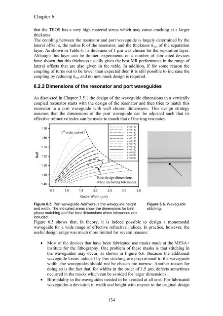
The coupling between the resonator and port waveguide is largely determined by the<br />
lateral offset s, the radius R of the resonator, and the thickness hsep of the separation<br />
layer. As shown in Table 6.1 a thickness of 1 µm was chosen for the separation layer.<br />
Although this layer can be thinner, experiments on a number of fabricated devices<br />
have shown that this thickness usually gives the best MR performance in the range of<br />
lateral offsets that are also given in the table. In addition, if for some reason the<br />
coupling of turns out to be lower than expected then it is still possible to increase the<br />
coupling by reducing hsep and no new mask design is required.<br />
6.2.2 Dimensions of the resonator and port waveguides<br />
As discussed in Chapter 3.5.1 the design of the waveguide dimensions in a vertically<br />
coupled resonator starts with the design of the resonator and then tries to match this<br />
resonator to a port waveguide with well chosen dimensions. This design strategy<br />
assumes that the dimensions of the port waveguide can be adjusted such that its<br />
effective refractive index can be made to match that of the ring resonator.<br />
Neff<br />
1.58<br />
1.56<br />
1.54<br />
1.52<br />
1.50<br />
1.48<br />
1.46<br />
0.5 1.0 1.5 2.0 2.5 3.0 3.5<br />
Guide Width (µm)<br />
134<br />
h = 0.110<br />
h = 0.120<br />
h = 0.130<br />
h = 0.140<br />
h = 0.150<br />
h = 0.160<br />
h = 0.170<br />
h = 0.180<br />
h = 0.190<br />
h = 0.200<br />
h = 0.220<br />
h = 0.260<br />
Figure 6.5. Port waveguide Neff versus the waveguide height<br />
and width. The indicated areas show the dimensions for best<br />
phase matching and the best dimensions when tolerances are<br />
included.<br />
1 st order cut-off<br />
Best design dimensions<br />
when including tolerances<br />
Figure 6.6. Waveguide<br />
stitching.<br />
Figure 6.5 shows that, in theory, it is indeed possible to design a monomodal<br />
waveguide for a wide range of effective refractive indices. In practice, however, the<br />
useful design range was much more limited for several reasons:<br />
• Most of the devices that have been fabricated use masks made at the MESA+<br />
institute for the lithography. One problem of these masks is that stitching in<br />
the waveguides may occur, as shown in Figure 6.6. Because the additional<br />
waveguide losses induced by this stitching are proportional to the waveguide<br />
width, the waveguides should not be chosen too narrow. Another reason for<br />
doing so is the fact that, for widths in the order of 1.5 µm, defects sometimes<br />
occurred in the masks which can be avoided for larger dimensions.<br />
• Bi-modality in the waveguides needed to be avoided at all cost. For fabricated<br />
waveguides a deviation in width and height with respect to the original design