- Page 1 and 2:
DENSELY INTEGRATED MICRORING- RESON
- Page 3 and 4:
DENSELY INTEGRATED MICRORING- RESON
- Page 5:
To my parents…
- Page 8 and 9:
esonators is limited by the spacing
- Page 10 and 11:
iv Samenvatting Dit proefschrift be
- Page 12 and 13:
schakelaar “aan” is, dan is de
- Page 14 and 15:
3.6.2 Overlap loss reduction.......
- Page 17 and 18:
Chapter 1 Introduction The devices
- Page 19 and 20:
1.2 Broadband to the home 3 Introdu
- Page 21 and 22:
1.3 Bringing Fiber to the Home 5 In
- Page 23 and 24:
Figure 1.5. The technological scope
- Page 25:
9 Introduction these basic paramete
- Page 28 and 29:
Chapter 2 2.1 Introduction Integrat
- Page 30 and 31:
Chapter 2 light Icav2 in the cavity
- Page 32 and 33:
Chapter 2 ∆ = ⎛ β r − β g
- Page 34 and 35:
Chapter 2 2.3.3 Combined model The
- Page 36 and 37:
Chapter 2 FC 4µ 1µ 2 ⋅ χr = 2
- Page 38 and 39:
Chapter 2 P Through /P In (dB) 0 -1
- Page 40 and 41:
Chapter 2 The figure shows that it
- Page 42 and 43:
Chapter 2 In − jϕr1 2 Figure 2.1
- Page 44 and 45:
Chapter 2 differences between the f
- Page 46 and 47:
Chapter 2 M = ⋅ FSR = N ⋅ FSR F
- Page 48 and 49:
Chapter 2 the heat will therefore f
- Page 50 and 51:
Chapter 2 index. Although this can
- Page 52 and 53:
Chapter 2 resonators for instance h
- Page 54 and 55:
Chapter 2 a rather complex MEMS bas
- Page 56 and 57:
Chapter 3 3.1 Introduction The most
- Page 58 and 59:
Chapter 3 3.2.1 Drop port on-resona
- Page 60 and 61:
Chapter 3 3.2.3 Filter bandwidth In
- Page 62 and 63:
Chapter 3 (resulting in a higher ba
- Page 64 and 65:
Chapter 3 Figure 3.11. Residual cha
- Page 66 and 67:
Chapter 3 3.3 Geometrical design ch
- Page 68 and 69:
Chapter 3 resonator and the port wa
- Page 70 and 71:
Chapter 3 Another important fact wh
- Page 72 and 73:
Chapter 3 The flowchart of the desi
- Page 74 and 75:
Chapter 3 While the resonator in th
- Page 76 and 77:
Chapter 3 3.6.1 Port waveguide and
- Page 78 and 79:
Chapter 3 overlap losses are only 0
- Page 80 and 81:
Chapter 3 3.7 Component design cons
- Page 82 and 83:
Chapter 3 By maximizing the power t
- Page 84 and 85:
Chapter 3 important, due to the fac
- Page 86 and 87:
Chapter 4 4.1 Introduction As was s
- Page 88 and 89:
Chapter 4 4.2.1 Transient response
- Page 90 and 91:
Chapter 4 Under the condition that
- Page 92 and 93: Chapter 4 Figure 4.4. Screenshot of
- Page 94 and 95: Chapter 4 The equations required to
- Page 96 and 97: Chapter 4 using an approach based o
- Page 98 and 99: Chapter 4 4.5.1 Architecture The Au
- Page 100 and 101: Chapter 4 4.5.2 Simulation method A
- Page 102 and 103: Chapter 4 Figure 4.9. A Primitive w
- Page 104 and 105: Chapter 4 Listing 4.3. Pseudo code
- Page 106 and 107: Chapter 4 Listing 4.4. Pseudo code
- Page 108 and 109: Chapter 4 simulated output spectra
- Page 110 and 111: Chapter 4 Figure 4.21. The reflecto
- Page 112 and 113: Chapter 4 P Drop /P In (dB) 0 -10 -
- Page 114 and 115: Chapter 4 Figure 4.27a. OADM with r
- Page 116 and 117: Chapter 4 will propagate through th
- Page 118 and 119: Chapter 4 As demonstrated by these
- Page 120 and 121: Chapter 4 What is more interesting
- Page 122 and 123: Chapter 4 method it does allow time
- Page 124 and 125: Chapter 4 complex than the interact
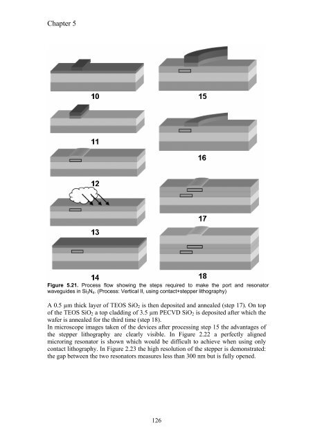
- Page 126 and 127: Chapter 5 5.1 Introduction The mate
- Page 128 and 129: Chapter 5 wafer is used (step 1). T
- Page 130 and 131: Chapter 5 range of 0.9 to 1.1 µm.
- Page 132 and 133: Chapter 5 The process flow with the
- Page 134 and 135: Chapter 5 5.3.3 Mask layout The big
- Page 136 and 137: Chapter 5 5.4. Fabrication and mask
- Page 138 and 139: Chapter 5 1. Definition of the vert
- Page 140 and 141: Chapter 5 5.4.2 Fabrication The fab
- Page 144 and 145: Chapter 5 removed using lift-off of
- Page 146 and 147: Chapter 6 6.1 Introduction About ha
- Page 148 and 149: Chapter 6 In early, comparatively s
- Page 150 and 151: Chapter 6 that the TEOS has a very
- Page 152 and 153: Chapter 6 The most important aspect
- Page 154 and 155: Chapter 6 6.2.3 Chromium heater des
- Page 156 and 157: Chapter 6 Therefore, even if the si
- Page 158 and 159: Chapter 6 Next, the heater was heat
- Page 160 and 161: Chapter 6 6.3 Characterization of s
- Page 162 and 163: Chapter 6 polarization maintaining
- Page 164 and 165: Chapter 6 the resonators in this gr
- Page 166 and 167: Chapter 6 Although the fitted coupl
- Page 168 and 169: Chapter 6 a cladding thickness of 3
- Page 170 and 171: Chapter 6 6.4 A wavelength selectiv
- Page 172 and 173: Chapter 6 A possible explanation fo
- Page 175 and 176: Chapter 7 Densely integrated device
- Page 177 and 178: Densely integrated devices for WDM-
- Page 179 and 180: Densely integrated devices for WDM-
- Page 181 and 182: Densely integrated devices for WDM-
- Page 183 and 184: 7.2.2 Spectral measurements Densely
- Page 185 and 186: Densely integrated devices for WDM-
- Page 187 and 188: Densely integrated devices for WDM-
- Page 189 and 190: Power Densely integrated devices fo
- Page 191 and 192: 7.3.4 Characterization Densely inte
- Page 193 and 194:
Densely integrated devices for WDM-
- Page 195 and 196:
Figure 7.31a. Eye pattern of the re
- Page 197:
Densely integrated devices for WDM-
- Page 200 and 201:
Chapter 8 8.1 Introduction In most
- Page 202 and 203:
Chapter 8 amount of power will be d
- Page 204 and 205:
Chapter 8 Another problem that may
- Page 206 and 207:
Chapter 8 halves that are each comp
- Page 209 and 210:
Chapter 9 Discussion and Conclusion
- Page 211 and 212:
Appendix A. Mason’s rule Several
- Page 213 and 214:
Appendix B. Crosstalk Derivation Th
- Page 215 and 216:
List of Acronyms ADSL - Asymmetric
- Page 217 and 218:
List of Symbols Q - Quality Factor
- Page 219 and 220:
Bibliography [1] Dan Schiller, “E
- Page 221 and 222:
Regions,” IEEE Photonics Technolo
- Page 223 and 224:
[66] B. E. Little, S. T. Chu, J. V.
- Page 225 and 226:
[97] H. Haeiwa, T. Naganawa and Y.
- Page 227 and 228:
[135] A. Driessen, D. H. Geuzebroek
- Page 229 and 230:
[165] T. Barwicz, M. R. Watts, M. A
- Page 231 and 232:
Publication List Patents (pending)
- Page 233 and 234:
R. Dekker, L.T.H.Hilderink, M.B.J.
- Page 235 and 236:
Networks (BB Photonics),” Interna
- Page 237 and 238:
Dankwoord/Acknowledgements Zo, dit
- Page 239:
223