Edwin Jan Klein - Universiteit Twente
Edwin Jan Klein - Universiteit Twente
Edwin Jan Klein - Universiteit Twente

Create successful ePaper yourself
Turn your PDF publications into a flip-book with our unique Google optimized e-Paper software.
145<br />
Microring-resonator building blocks<br />
on a 50 µm wide multi mode fiber. The light is then measured using a HP 81521B<br />
photo-detector.<br />
Aside from the measurements with the tunable laser this setup was also used in<br />
combination with a Sensors Unlimited 320 MX-1.7 RT infrared camera. The camera<br />
provides unique information that cannot be obtained through other means, e.g. by<br />
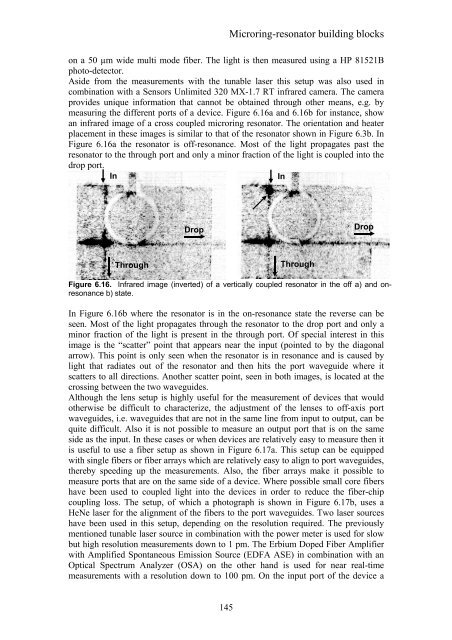
measuring the different ports of a device. Figure 6.16a and 6.16b for instance, show<br />
an infrared image of a cross coupled microring resonator. The orientation and heater<br />
placement in these images is similar to that of the resonator shown in Figure 6.3b. In<br />
Figure 6.16a the resonator is off-resonance. Most of the light propagates past the<br />
resonator to the through port and only a minor fraction of the light is coupled into the<br />
drop port.<br />
In In<br />
Through<br />
Drop<br />
Through<br />
Drop<br />
Figure 6.16. Infrared image (inverted) of a vertically coupled resonator in the off a) and onresonance<br />
b) state.<br />
In Figure 6.16b where the resonator is in the on-resonance state the reverse can be<br />
seen. Most of the light propagates through the resonator to the drop port and only a<br />
minor fraction of the light is present in the through port. Of special interest in this<br />
image is the “scatter” point that appears near the input (pointed to by the diagonal<br />
arrow). This point is only seen when the resonator is in resonance and is caused by<br />
light that radiates out of the resonator and then hits the port waveguide where it<br />
scatters to all directions. Another scatter point, seen in both images, is located at the<br />
crossing between the two waveguides.<br />
Although the lens setup is highly useful for the measurement of devices that would<br />
otherwise be difficult to characterize, the adjustment of the lenses to off-axis port<br />
waveguides, i.e. waveguides that are not in the same line from input to output, can be<br />
quite difficult. Also it is not possible to measure an output port that is on the same<br />
side as the input. In these cases or when devices are relatively easy to measure then it<br />
is useful to use a fiber setup as shown in Figure 6.17a. This setup can be equipped<br />
with single fibers or fiber arrays which are relatively easy to align to port waveguides,<br />
thereby speeding up the measurements. Also, the fiber arrays make it possible to<br />
measure ports that are on the same side of a device. Where possible small core fibers<br />
have been used to coupled light into the devices in order to reduce the fiber-chip<br />
coupling loss. The setup, of which a photograph is shown in Figure 6.17b, uses a<br />
HeNe laser for the alignment of the fibers to the port waveguides. Two laser sources<br />
have been used in this setup, depending on the resolution required. The previously<br />
mentioned tunable laser source in combination with the power meter is used for slow<br />
but high resolution measurements down to 1 pm. The Erbium Doped Fiber Amplifier<br />
with Amplified Spontaneous Emission Source (EDFA ASE) in combination with an<br />
Optical Spectrum Analyzer (OSA) on the other hand is used for near real-time<br />
measurements with a resolution down to 100 pm. On the input port of the device a