Edwin Jan Klein - Universiteit Twente
Edwin Jan Klein - Universiteit Twente
Edwin Jan Klein - Universiteit Twente

You also want an ePaper? Increase the reach of your titles
YUMPU automatically turns print PDFs into web optimized ePapers that Google loves.
Chapter 5<br />
5.4. Fabrication and mask design of vertically coupled<br />
resonators defined using stepper lithography<br />
5.4.1 Stepper lithography and mask design<br />
As pointed out in the previous section, only 1/36 th of the total number of fabricated<br />
devices can be properly aligned when building cross-coupled micro-resonators using<br />
contact lithography. This is not necessarily a problem when small devices, consisting<br />
of one or two microring-resonators, are built. Assuming a realistic average device<br />
height of 500 µm then, when using 6 columns, 20 devices can fit in the 1 cm 2 area<br />
allotted to a single group. Because the devices are, on average, only 1.5 mm in width<br />
(largely due to bends, tapers etc), the number of columns can even be tripled to 18,<br />
giving a total number of 60 functional devices per wafer, which gives more than<br />
enough devices for redundancy and parameter variations. More complex devices such<br />
as for instance the later discussed OADM and λ-Router, have a height between 1.5<br />
and 2 mm and a width of about 5 mm. At most 10 to 12 of these devices can therefore<br />
be put on 1 cm 2 which leaves almost no room for redundancy. Considering the fact<br />
that inevitably some of these devices will be damaged during fabrication [132],<br />
getting sufficient yield (or even functional devices) can be a problem.<br />
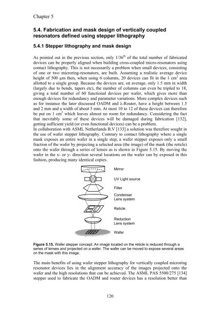
In collaboration with ASML Netherlands B.V [133] a solution was therefore sought in<br />
the use of wafer stepper lithography. Contrary to contact lithography where a single<br />
mask exposes an entire wafer in a single step, a wafer stepper exposes only a small<br />
fraction of the wafer by projecting a selected area (the image) of the mask (the reticle)<br />
onto the wafer through a series of lenses as is shown in Figure 5.15. By moving the<br />
wafer in the x- or y- direction several locations on the wafer can by exposed in this<br />
fashion, producing many identical copies.<br />
Figure 5.15. Wafer stepper concept: An image located on the reticle is reduced through a<br />
series of lenses and projected on a wafer. The wafer can be moved to expose several areas<br />
on the mask with this image.<br />
The main benefits of using wafer stepper lithography for vertically coupled microring<br />
resonator devices lies in the alignment accuracy of the images projected onto the<br />
wafer and the high resolutions that can be achieved. The ASML PAS 5500/275 [134]<br />
stepper used to fabricate the OADM and router devices has a resolution better than<br />
120<br />
Mirror<br />
UV Light source<br />
Filter<br />
Condenser<br />
Lens system<br />
Reticle<br />
Reduction<br />
Lens system<br />
Wafer