MPLAB ICD 3 In-Circuit Debugger User's Guide
MPLAB ICD 3 In-Circuit Debugger User's Guide
MPLAB ICD 3 In-Circuit Debugger User's Guide
- No tags were found...

Create successful ePaper yourself
Turn your PDF publications into a flip-book with our unique Google optimized e-Paper software.
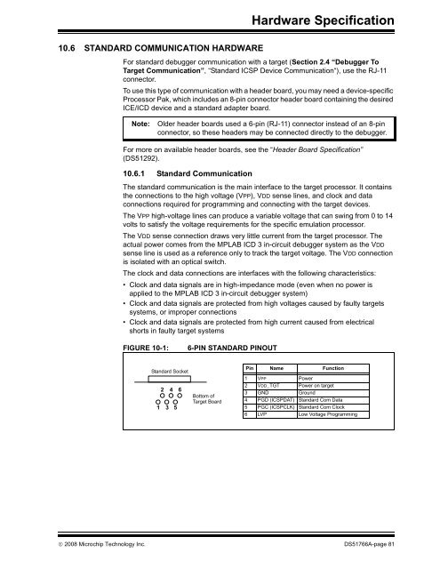
Hardware Specification10.6 STANDARD COMMUNICATION HARDWAREFor standard debugger communication with a target (Section 2.4 “<strong>Debugger</strong> ToTarget Communication”, “Standard ICSP Device Communication“), use the RJ-11connector.To use this type of communication with a header board, you may need a device-specificProcessor Pak, which includes an 8-pin connector header board containing the desiredICE/<strong>ICD</strong> device and a standard adapter board.Note:Older header boards used a 6-pin (RJ-11) connector instead of an 8-pinconnector, so these headers may be connected directly to the debugger.For more on available header boards, see the “Header Board Specification”(DS51292).10.6.1 Standard CommunicationThe standard communication is the main interface to the target processor. It containsthe connections to the high voltage (VPP), VDD sense lines, and clock and dataconnections required for programming and connecting with the target devices.The VPP high-voltage lines can produce a variable voltage that can swing from 0 to 14volts to satisfy the voltage requirements for the specific emulation processor.The VDD sense connection draws very little current from the target processor. Theactual power comes from the <strong>MPLAB</strong> <strong>ICD</strong> 3 in-circuit debugger system as the VDDsense line is used as a reference only to track the target voltage. The VDD connectionis isolated with an optical switch.The clock and data connections are interfaces with the following characteristics:• Clock and data signals are in high-impedance mode (even when no power isapplied to the <strong>MPLAB</strong> <strong>ICD</strong> 3 in-circuit debugger system)• Clock and data signals are protected from high voltages caused by faulty targetssystems, or improper connections• Clock and data signals are protected from high current caused from electricalshorts in faulty target systemsFIGURE 10-1:6-PIN STANDARD PINOUTStandard Socket123456Bottom ofTarget BoardPin Name Function1 VPP Power2 VDD_TGT Power on target3 GND Ground4 PGD (ICSPDAT) Standard Com Data5 PGC (ICSPCLK) Standard Com Clock6 LVP Low Voltage Programming© 2008 Microchip Technology <strong>In</strong>c. DS51766A-page 81