- Page 1 and 2:
®Established 1981Advanced Test Equ
- Page 3 and 4:
WARRANTYKeithley Instruments, Inc.
- Page 5 and 6:
Manual Print HistoryThe print histo
- Page 7 and 8:
If you are using a test fixture, ke
- Page 9 and 10:
Table of Contents1 General Informat
- Page 11 and 12:
4.10.3 Scanning examples ..........
- Page 13:
5.13.4 :FCHannels ................
- Page 16 and 17:
List of Illustrations2 Card Install
- Page 18 and 19:
6 Theory of OperationFigure 6-1 Mod
- Page 20 and 21:
8 MaintenanceTable 8-1Table 8-2Tabl
- Page 22 and 23:
General Informationthorized repair
- Page 24 and 25:
Card InstallationNOTEIf using the s
- Page 26 and 27:
3Getting Started3.1 IntroductionThi
- Page 28 and 29:
Getting StartedWARNING: INTERCONNEC
- Page 30 and 31:
Getting StartedSLOT 112ROW34COLUMN
- Page 32 and 33:
Getting Started3.6 Overview of scan
- Page 34 and 35:
Getting Started3.7.2 Close and open
- Page 36 and 37:
Getting Started2. If the scan list
- Page 38 and 39:
Getting Started3.8 Switching card c
- Page 40 and 41:
Getting Started3.9.2 Close and Open
- Page 42 and 43:
Getting StartedSCPI (Standard Comma
- Page 44 and 45:
Getting Started3.10.5 Abbreviated s
- Page 46 and 47:
Getting Started20 OUTPUT 707; “:s
- Page 48 and 49:
4Front Panel Operation4.1 Introduct
- Page 50 and 51:
Front Panel OperationAnnunciatorsTa
- Page 52 and 53:
Front Panel Operation3COLUMNSLOT 1
- Page 54 and 55:
Front Panel OperationNot all Model
- Page 56 and 57:
Front Panel Operationthe VFD which
- Page 58 and 59:
Front Panel OperationFront panel ke
- Page 60 and 61:
Front Panel OperationSlot 111 2 3 4
- Page 62 and 63:
Front Panel Operation4.8 Channel li
- Page 64 and 65:
Front Panel OperationStep 3. Enter
- Page 66 and 67:
Front Panel Operationd. Click the I
- Page 68 and 69:
Front Panel OperationIdleOPEN ALLId
- Page 70 and 71:
Front Panel OperationChannel layerN
- Page 72 and 73:
Front Panel Operationsatisfy a chan
- Page 74 and 75:
Front Panel OperationExample 3:ARM
- Page 76 and 77:
Front Panel Operation6. To store th
- Page 78 and 79:
Front Panel Operation8. The INFO ke
- Page 80 and 81:
Front Panel Operation4.12.2 GPIBThe
- Page 82 and 83:
Front Panel OperationPerform the fo
- Page 84 and 85:
Front Panel OperationPlace the curs
- Page 86 and 87:
Front Panel OperationThe message in
- Page 88 and 89:
Front Panel Operation4.14 Scan conf
- Page 90 and 91:
Front Panel OperationTable 4-7 (con
- Page 92 and 93:
Front Panel Operationline. Perform
- Page 94 and 95:
Front Panel Operation2. To retain t
- Page 96 and 97:
Front Panel OperationPerform the fo
- Page 98 and 99:
Front Panel Operation4.14.4 Channel
- Page 100 and 101:
Front Panel Operation3. Interlocked
- Page 102 and 103:
Front Panel OperationPin 7 - Digita
- Page 104 and 105:
Front Panel OperationCHANNELREADY4.
- Page 106 and 107:
Front Panel OperationFor this test
- Page 108 and 109:
Front Panel OperationDUT#11OUTPUTDU
- Page 110 and 111:
Front Panel OperationBypass7002Pres
- Page 112 and 113:
Front Panel OperationDUT#11OUTPUTHI
- Page 114 and 115:
Front Panel Operation7002Press STEP
- Page 116 and 117:
Front Panel OperationINOUTTriggerLi
- Page 118 and 119:
Front Panel Operationmeter to measu
- Page 120 and 121:
5IEEE-488 Reference5.1 Introduction
- Page 122 and 123:
IEEE-488 ReferenceIEEE-488Table 5-1
- Page 124 and 125:
IEEE-488 ReferenceNOTEController pr
- Page 126 and 127:
IEEE-488 ReferenceTriggerTransition
- Page 128 and 129:
IEEE-488 ReferenceStandard Event St
- Page 130 and 131:
IEEE-488 ReferenceThe filter can be
- Page 132 and 133:
IEEE-488 ReferenceArm Condition Reg
- Page 134 and 135:
IEEE-488 ReferenceAlwaysZeroLay2Lay
- Page 136 and 137:
IEEE-488 ReferenceAlwaysZeroSeq1(B1
- Page 138 and 139:
IEEE-488 Reference5.6.6 Questionabl
- Page 140 and 141:
IEEE-488 ReferenceReading this regi
- Page 142 and 143:
IEEE-488 ReferenceB6 is called the
- Page 144:
IEEE-488 Reference:ABORt*RST:SYST:P
- Page 147 and 148:
IEEE-488 ReferenceWith the Manual c
- Page 149 and 150:
IEEE-488 Reference5.8.2 IFC (interf
- Page 151 and 152:
IEEE-488 Reference5-32
- Page 153:
IEEE-488 Reference• While ignorin
- Page 156 and 157:
IEEE-488 Referenceas command paths.
- Page 158 and 159:
IEEE-488 ReferenceResponse messages
- Page 160 and 161:
IEEE-488 Reference5.10 Common comma
- Page 162 and 163:
IEEE-488 Reference5.10.1 *CLS ⎯ c
- Page 164 and 165:
IEEE-488 Referencewhere; CME (bit B
- Page 166 and 167:
IEEE-488 Reference5.10.4 *ESR? ⎯
- Page 168 and 169:
IEEE-488 Reference5.10.5 *IDN? ⎯
- Page 170 and 171:
IEEE-488 ReferenceNOTESee *OPC?, *T
- Page 172 and 173:
IEEE-488 ReferenceAfter *OPC? is ex
- Page 174 and 175:
IEEE-488 Reference5.10.9 *RCL ⎯ r
- Page 176 and 177:
IEEE-488 ReferenceTable 5-5Default
- Page 178 and 179:
IEEE-488 Reference5.10.12 *SRE ⎯
- Page 180 and 181:
IEEE-488 Reference5.10.13 *SRE? ⎯
- Page 182 and 183:
IEEE-488 ReferenceBit 5, Event Summ
- Page 184 and 185:
IEEE-488 Reference5.10.16 *TST? ⎯
- Page 186 and 187:
IEEE-488 ReferenceLine 70 Wait unti
- Page 188 and 189:
IEEE-488 ReferenceSCPI command subs
- Page 190 and 191:
IEEE-488 Reference5.11 :DISPlay sub
- Page 192 and 193:
:DISPlay subsystemIEEE-488 Referenc
- Page 194 and 195:
:DISPlay subsystemIEEE-488 Referenc
- Page 196 and 197:
IEEE-488 Reference5.12 :OUTPut subs
- Page 198 and 199:
IEEE-488 Reference5.13 [:ROUTe] sub
- Page 200 and 201:
[:ROUTe] subsystemIEEE-488 Referenc
- Page 202 and 203:
[:ROUTe] subsystemIEEE-488 Referenc
- Page 204 and 205:
[:ROUTe] subsystemIEEE-488 Referenc
- Page 206 and 207:
[:ROUTe] subsystemIEEE-488 Referenc
- Page 208 and 209:
[:ROUTe] subsystemIEEE-488 Referenc
- Page 210 and 211:
[:ROUTe] subsystemIEEE-488 Referenc
- Page 212 and 213:
[:ROUTe] subsystemIEEE-488 Referenc
- Page 214 and 215:
[:ROUTe] subsystemIEEE-488 Referenc
- Page 216 and 217:
[:ROUTe] subsystemIEEE-488 Referenc
- Page 218 and 219:
IEEE-488 Reference5.14 Sense subsys
- Page 220 and 221:
IEEE-488 Reference5.15 :SOURce subs
- Page 222 and 223: IEEE-488 Reference5.16 :STATus subs
- Page 224 and 225: :STATus SubsystemIEEE-488 Reference
- Page 226 and 227: :STATus SubsystemIEEE-488 Reference
- Page 228 and 229: :STATus SubsystemIEEE-488 Reference
- Page 230 and 231: :STATus SubsystemIEEE-488 Reference
- Page 232 and 233: :STATus SubsystemIEEE-488 Reference
- Page 234 and 235: :STATus SubsystemIEEE-488 Reference
- Page 236 and 237: :STATus SubsystemIEEE-488 Reference
- Page 238 and 239: :STATus SubsystemIEEE-488 Reference
- Page 240 and 241: :STATus SubsystemIEEE-488 Reference
- Page 242 and 243: :STATus SubsystemIEEE-488 Reference
- Page 244 and 245: :STATus SubsystemIEEE-488 Reference
- Page 246 and 247: IEEE-488 Reference5.17 :SYSTem subs
- Page 248 and 249: :SYSTem SubsystemIEEE-488 Reference
- Page 250 and 251: IEEE-488 Reference5.18 Trigger subs
- Page 252 and 253: Trigger subsystemIEEE-488 Reference
- Page 254 and 255: Trigger subsystemIEEE-488 Reference
- Page 256 and 257: Trigger subsystemIEEE-488 Reference
- Page 258 and 259: Trigger subsystemIEEE-488 Reference
- Page 260 and 261: Trigger subsystemIEEE-488 Reference
- Page 262 and 263: Trigger subsystemIEEE-488 Reference
- Page 264 and 265: Trigger subsystemIEEE-488 Reference
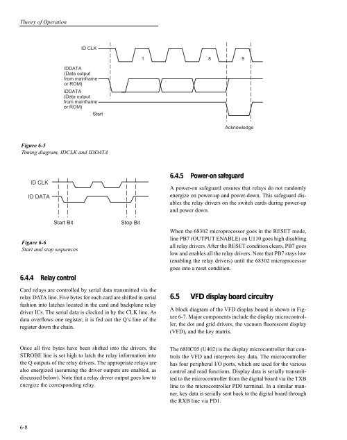
- Page 266 and 267: 6Theory of Operation6.1 Introductio
- Page 268 and 269: Theory of Operation6.3 Control func
- Page 270 and 271: Theory of Operation6.4 Relay contro
- Page 274 and 275: Theory of OperationFromDigitalBoard
- Page 276 and 277: Theory of Operationµ DINConnectorT
- Page 278 and 279: MaintenanceNOTEThe digital and disp
- Page 280 and 281: MaintenanceFuse replacement procedu
- Page 282 and 283: Maintenance7.6 Instrument disassemb
- Page 284 and 285: Maintenance7.6.5 Power supplies rem
- Page 286 and 287: Maintenance8. Press “1”, “1
- Page 288 and 289: MaintenanceEDIT ERR REM TALK LSTN S
- Page 290 and 291: MaintenanceTo review the error, pre
- Page 292 and 293: MaintenanceTrigger 8 (STI8) is set
- Page 294 and 295: MaintenanceDETAIL AREF:GRN/YELWIRE#
- Page 296 and 297: MaintenanceBOARDS MUST BE HANDLED W
- Page 298 and 299: MaintenanceSTEP 1FA-151-1, FASTENER
- Page 300 and 301: MaintenanceDETAIL ACC-47, CABLEDIG
- Page 302 and 303: Maintenance8#4-40x1/4"PFH(4 REQ'D)(
- Page 304 and 305: Replaceable Parts
- Page 306 and 307: Replaceable Parts
- Page 311 and 312: Replaceable PartsTable 8-2Digital b
- Page 313 and 314: Artisan Scientific - Quality Instru
- Page 315: (+5V)**(+5V)**** ****** **********
- Page 318 and 319: Replaceable PartsTable 8-3VFD displ
- Page 322 and 323:
Replaceable PartsTable 8-4Backplane
- Page 324:
Artisan Scientific - Quality Instru
- Page 327 and 328:
Replaceable Parts
- Page 331 and 332:
Replaceable PartsTable 8-6Miscellan
- Page 333 and 334:
Interface Function CodesTable A-1Mo
- Page 335 and 336:
Controller ProgramsIBM PC/XT/AT wit
- Page 337 and 338:
Controller Programs10 DEF SEG=&HC40
- Page 339 and 340:
Controller ProgramsHewlett-Packard
- Page 341 and 342:
Controller ProgramsBUS.INIT\ Initia
- Page 343 and 344:
CASCII Character Codesand IEEE-488
- Page 345 and 346:
ASCII Character Codes and IEEE-488M
- Page 347 and 348:
IEEE-488 Bus Overviewtype of instru
- Page 349 and 350:
IEEE-488 Bus Overviewdevice will re
- Page 351 and 352:
IEEE-488 Bus OverviewLAG (Listen Ad
- Page 353 and 354:
IEEE-488 Bus OverviewTable D-2Hexad
- Page 355 and 356:
EIEEE-488 Conformance InformationIn
- Page 357 and 358:
FSCPI Conformance InformationIntrod
- Page 359 and 360:
SCPI Conformance InformationTable F
- Page 361 and 362:
SCPI Conformance InformationTable F
- Page 363 and 364:
SCPI Conformance InformationTable F
- Page 365 and 366:
IEEE-488.2 Common CommandsMnemonic
- Page 367 and 368:
SCPI Command SubsystemTable H-1DISP
- Page 369 and 370:
SCPI Command SubsystemTable H-4SENS
- Page 371 and 372:
SCPI Command SubsystemTable H-6 (co
- Page 373 and 374:
SCPI Command SubsystemTable H-8 (co
- Page 375 and 376:
QuickBasic and QuickC ProgramsMicro
- Page 377 and 378:
QuickBasic and QuickC ProgramsMicro
- Page 379 and 380:
Index:ABORt 5-134:BBMake 5-88:CLOS
- Page 381 and 382:
Scanning channels 4-20Scanning exam
- Page 383:
Specifications are subject to chang