Navy Electricity and Electronics Training Series - Historic Naval ...
Navy Electricity and Electronics Training Series - Historic Naval ...
Navy Electricity and Electronics Training Series - Historic Naval ...

Create successful ePaper yourself
Turn your PDF publications into a flip-book with our unique Google optimized e-Paper software.
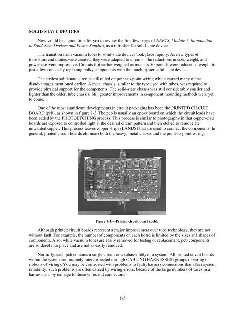
SOLID-STATE DEVICESNow would be a good time for you to review the first few pages of NEETS, Module 7, Introductionto Solid-State Devices <strong>and</strong> Power Supplies, as a refresher for solid-state devices.The transition from vacuum tubes to solid-state devices took place rapidly. As new types oftransistors <strong>and</strong> diodes were created, they were adapted to circuits. The reductions in size, weight, <strong>and</strong>power use were impressive. Circuits that earlier weighed as much as 50 pounds were reduced in weight tojust a few ounces by replacing bulky components with the much lighter solid-state devices.The earliest solid-state circuits still relied on point-to-point wiring which caused many of thedisadvantages mentioned earlier. A metal chassis, similar to the type used with tubes, was required toprovide physical support for the components. The solid-state chassis was still considerably smaller <strong>and</strong>lighter than the older, tube chassis. Still greater improvements in component mounting methods were yetto come.One of the most significant developments in circuit packaging has been the PRINTED CIRCUITBOARD (pcb), as shown in figure 1-3. The pcb is usually an epoxy board on which the circuit leads havebeen added by the PHOTOETCHING process. This process is similar to photography in that copper-cladboards are exposed to controlled light in the desired circuit pattern <strong>and</strong> then etched to remove theunwanted copper. This process leaves copper strips (LANDS) that are used to connect the components. Ingeneral, printed circuit boards eliminate both the heavy, metal chassis <strong>and</strong> the point-to-point wiring.Figure 1-3.—Printed circuit board (pcb).Although printed circuit boards represent a major improvement over tube technology, they are notwithout fault. For example, the number of components on each board is limited by the sizes <strong>and</strong> shapes ofcomponents. Also, while vacuum tubes are easily removed for testing or replacement, pcb componentsare soldered into place <strong>and</strong> are not as easily removed.Normally, each pcb contains a single circuit or a subassembly of a system. All printed circuit boardswithin the system are routinely interconnected through CABLING HARNESSES (groups of wiring orribbons of wiring). You may be confronted with problems in faulty harness connections that affect systemreliability. Such problems are often caused by wiring errors, because of the large numbers of wires in aharness, <strong>and</strong> by damage to those wires <strong>and</strong> connectors.1-5