- Page 1 and 2: NONRESIDENTTRAININGCOURSESEPTEMBER
- Page 3 and 4: PREFACEBy enrolling in this self-st
- Page 5: TABLE OF CONTENTSCHAPTERPAGE1. Micr
- Page 8 and 9: Module 11, Microwave Principles, ex
- Page 10 and 11: INSTRUCTIONS FOR TAKING THE COURSEA
- Page 12 and 13: THIS PAGE LEFT BLANK INTENTIONALLY.
- Page 15 and 16: CHAPTER 1MICROELECTRONICSLEARNING O
- Page 17 and 18: VACUUM-TUBE EQUIPMENTVacuum tubes w
- Page 19 and 20: SOLID-STATE DEVICESNow would be a g
- Page 21 and 22: FILM INTEGRATED CIRCUITS are broken
- Page 23 and 24: Development of a microelectronic de
- Page 25 and 26: Figure 1-9.—Crystal furnace.The c
- Page 27 and 28: Figure 1-12.—Planar-diffused tran
- Page 29 and 30: Figure 1-14.—Vacuum evaporation o
- Page 31 and 32: Figure 1-17.—Cathode-sputtering m
- Page 33 and 34: Q23. How do the two types of monoli
- Page 35 and 36: Figure 1-21A.—TO-5 mounting PLUG-
- Page 37 and 38: Dual Inline PackageThe dual inline
- Page 39 and 40: wafer, as shown in figure 1-27. Thi
- Page 41 and 42: Figure 1-29.—J-K flip-flop discre
- Page 43 and 44: Figure 1-31.—Lead numbering for a
- Page 45 and 46: Figure 1-34.—Manufacturer's Data
- Page 47: comparison to the distance between
- Page 52 and 53: Conductors located several layers b
- Page 54 and 55: Figure 1-43A.—Evolution of modula
- Page 56 and 57: ENVIRONMENTAL CONSIDERATIONSThe env
- Page 58 and 59: SUMMARYThis topic has presented inf
- Page 60 and 61: Rapid development has resulted in i
- Page 62 and 63: Large DIPs are being used to packag
- Page 64 and 65: MINIATURE ELECTRONICS are card asse
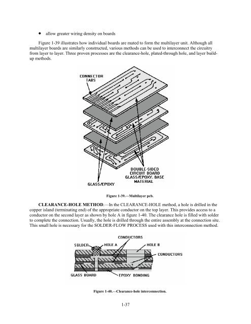
- Page 66 and 67: Three methods of interconnecting ci
- Page 68 and 69: ANSWERS TO QUESTIONS Q1. THROUGH Q5
- Page 70 and 71: A43. Conventional printed circuit b
- Page 72 and 73: Upon satisfactory completion of a 2
- Page 74 and 75: One such improvement in system test
- Page 76 and 77: those that should be observed when
- Page 78 and 79: Figure 2-2.—Low voltage Handpiece
- Page 80 and 81: Figure 2-6.—Rotary-drive machine
- Page 82 and 83: Figure 2-9.—Pana Vise.HAND TOOLSF
- Page 84 and 85: Figure 2-10a.—Pliers.TweezersView
- Page 86 and 87: Even though all the items are not u
- Page 88 and 89: Figure 2-14.—Stereoscopic zoom mi
- Page 90 and 91: other than eutectic, go through a p
- Page 92 and 93: A1. Chief of Naval Operations (CNO)
- Page 94 and 95: CAUTIONTHIS SECTION IS NOT, IN ANY
- Page 96 and 97: The coating material can best be id
- Page 98 and 99: Figure 3-3.—Rotary tool conformal
- Page 100 and 101:
Figure 3-4A.—Eyelets (interfacial
- Page 102 and 103:
Figure 3-5B.—Clinched leads. SEMI
- Page 104 and 105:
Figure 3-8A.—Terminals. PIN AND T
- Page 106 and 107:
Figure 3-8E.—Terminals. SOLDER CU
- Page 108 and 109:
Figure 3-10.—Solder wicking.This
- Page 110 and 111:
Figure 3-12B.—Motorized vacuum/pr
- Page 112 and 113:
INSTALLATION AND SOLDERING OF PRINT
- Page 114 and 115:
Figure 3-15.—Component arrangemen
- Page 116 and 117:
Figure 3-16.—Thermal shunt.APPLIC
- Page 118 and 119:
Removal of Plug-In DIPsTo remove pl
- Page 120 and 121:
Figure 3-19.—TO mounting techniqu
- Page 122 and 123:
Figure 3-21.—Flat pack in protect
- Page 124 and 125:
Figure 3-23.—Pcb conductor damage
- Page 126 and 127:
REPAIRING DELAMINATED CONDUCTORS.
- Page 128 and 129:
5. The repair is completed using th
- Page 130 and 131:
SAFETYSafety is a subject of utmost
- Page 132 and 133:
OBJECT OR PROCESSWORK SURFACESFLOOR
- Page 134 and 135:
8. When moving an ESDS device or as
- Page 136 and 137:
Power ToolsHazards associated with
- Page 138 and 139:
dispensers will prevent many accide
- Page 140 and 141:
A GOOD SOLDER JOINT is bright and s
- Page 142 and 143:
ANSWERS TO QUESTIONS Q1. THROUGH Q3
- Page 145 and 146:
APPENDIX IGLOSSARYALLOWANCE PARTS L
- Page 147 and 148:
MODULAR PACKAGING—Circuit assembl
- Page 149:
APPENDIX IIREFERENCE LISTCHAPTER ON
- Page 152 and 153:
Microelectronics—Continuedpackagi
- Page 155:
Assignment QuestionsInformation: Th
- Page 158 and 159:
1-7. Which of the following charact
- Page 160 and 161:
1-24. Vacuum evaporation and cathod
- Page 162 and 163:
___________________________________
- Page 164 and 165:
1-49. Ground planes and shielding a
- Page 166 and 167:
1-65. Which of the following types
- Page 168 and 169:
ASSIGNMENT 2Textbook assignment: Ch
- Page 170 and 171:
2-20. Turret, fork, and hook termin
- Page 172 and 173:
2-39. Component leads may be clippe
- Page 174 and 175:
2-52. To ensure a good mechanical b