NASA Scientific and Technical Aerospace Reports
NASA Scientific and Technical Aerospace Reports
NASA Scientific and Technical Aerospace Reports

Create successful ePaper yourself
Turn your PDF publications into a flip-book with our unique Google optimized e-Paper software.
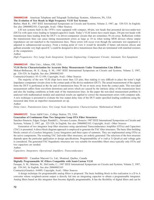
20060002148 American Telephone <strong>and</strong> Telegraph Technology Systems, Allentown, PA, USA<br />
The Evolution of Test Heads in High Frequency VLSI Test Systems<br />
Barber, Mark R.; 1987 IEEE International Symposium on Circuits <strong>and</strong> Systems, Volume 2; 1987, pp. 520-525; In English;<br />
See also 20060002103; Copyright; Avail.: Other Sources<br />
LSI test systems built in the 1970’s were equipped with compact, 60-pin, test heads that presented devices-under-test<br />
(DUT)s with open wires leading to lumped-capacitive loads. Today’s VLSI testers have much larger, 256-pin test heads with<br />
transmission lines leading from the DUT’s to driver-comparator circuits that are sometimes 50 cm away. Reflections within<br />
the transmission lines can cause timing measurement errors as large as 10 ns when testing MOS devices whose output<br />
impedances are not matched to the transmission lines. These errors will occur even though the automatic test equipment is<br />
adjusted to subnanosecond accuracy. From a testing point of view it would be desirable if future sub-micron silicon <strong>and</strong><br />
gallium arsenide very high speed IC’s could be designed to drive transmission lines that are terminated with matched resistors<br />
at the comparators.<br />
Author<br />
High Frequencies; Very Large Scale Integration; Systems Engineering; Comparator Circuits; Automatic Test Equipment<br />
20060002149 Ohio Univ., Athens, OH, USA<br />
VLSI Device Characterization for Accurate Delay Measurements Under Transmission Line Effects<br />
Mokari-Bolhassan, M. E.; Kang, S. M.; 1987 IEEE International Symposium on Circuits <strong>and</strong> Systems, Volume 2; 1987,<br />
pp. 526-529; In English; See also 20060002103<br />
Contract(s)/Grant(s): 85-12-109; Copyright; Avail.: Other Sources<br />
The majority of the new VLSI chips have more than 125 pins, thus making it very difficult to place the tester’s high<br />
impedance comparator circuits close to the contact pads of the device-undertest (DUT). The actual measurement of the signals<br />
form the DUT is performed at the far end of transmission lines 50 cm or more away from the contact pads. This non-ideal<br />
measurement suffers from waveform distortions <strong>and</strong> errors which are caused by the intrinsic delay of the transmission lines<br />
<strong>and</strong> also the loading conditions at both ends of the transmission lines. In this paper the non-ideal measurement problem Is<br />
analyzed with mathematical mode]s <strong>and</strong> analytical results are applied to correct the measurement errors with computer aids.<br />
A new technique is presented to evaluate the true output delay time of the DUT under specified loading conditions using the<br />
measured data from an imperfect measurement set up.<br />
Author<br />
Delay Lines; Transmission Lines; Very Large Scale Integration; Characterization; Mathematical Models<br />
20060002152 Texas A&M Univ., College Station, TX, USA<br />
Generation of Continuous-Time Two Integrator Loop OTA Filter Structures<br />
Sanchez-Sinencio, Edgar; Geiger, R<strong>and</strong>all L.; Nevarez-Lozano, Horacio; 1987 IEEE International Symposium on Circuits <strong>and</strong><br />
Systems, Volume 2; 1987, pp. 325-328; In English; See also 20060002103; Copyright; Avail.: Other Sources<br />
Generation of two integrator loop filter structures using operational Transconductance Amplifier (OTAs) <strong>and</strong> Capacitors<br />
(TAC) is presented. A direct block diagram approach is employed to generate the TAC filter structures. The basic filter building<br />
blocks consist of a Lossless Integrator, Lossy Integrators <strong>and</strong> three types of summers. They are implemented using OTAs as<br />
the active components. The resulting TAC 2nd-order filter structures, are orderly generated. The selection of the best structure<br />
depends upon the particular application or design specifications. Programmability of w (sub p 3) Q(sub p) <strong>and</strong> voltage gain<br />
is considered. The generated TAC biquadratic structures are very suitable for monolithic filters since typically only OTAs <strong>and</strong><br />
two capacitors are needed.<br />
Author<br />
Capacitors; Integrators; Operational Amplifiers; Transconductance<br />
20060002153 Canadian Marconi Co. Ltd., Montreal, Quebec, Canada<br />
Digitally Programmable SC-Filters Compatible with Semi-Custom VLSI<br />
Faruque, S. M.; Martens, W.; DeCombe, C.; 1987 IEEE International Symposium on Circuits <strong>and</strong> Systems, Volume 2; 1987,<br />
pp. 339-341; In English; See also 20060002103<br />
Contract(s)/Grant(s): A4489; Copyright; Avail.: Other Sources<br />
A design technique for programmable analog filters is proposed. The basic building block in this realization is aDtoA<br />
converter whose weighted-current output is directly fed into an integrating capacitor to obtain a programmable integrator.<br />
Analog filters based on this integrator then become digitally programmable, It has the flexibility of digital filters <strong>and</strong> can be<br />
72