- Page 2 and 3:
Characteristics of Selected Element
- Page 5 and 6:
With WileyPLUS: This online teachin
- Page 7 and 8:
E IGHTH E DITION Materials Science
- Page 9:
Dedicated to our wives, Nancy and E
- Page 12 and 13:
viii • Preface FEATURES THAT ARE
- Page 14 and 15:
x • Preface 2. Answers to Concept
- Page 16 and 17:
Appreciation is expressed to those
- Page 18 and 19:
xiv • Contents 3. The Structure o
- Page 20 and 21:
xvi • Contents 9.12 Development o
- Page 22 and 23:
xviii • Contents 15.14 Factors Th
- Page 24 and 25:
xx • Contents 21.14 Optical Fiber
- Page 26 and 27:
xxii • List of Symbols HK Knoop
- Page 29 and 30:
Chapter 1 Introduction A familiar i
- Page 31 and 32:
1.2 Materials Science and Engineeri
- Page 33 and 34:
1.4 Classification of Materials •
- Page 35 and 36:
1.4 Classification of Materials •
- Page 37 and 38:
1.4 Classification of Materials •
- Page 39 and 40:
1.5 Advanced Materials • 11 aeros
- Page 41 and 42:
1.6 Modern Materials’ Needs • 1
- Page 43 and 44:
STEELS Processing Diffusion ➣ Rec
- Page 45 and 46:
Question • 17 REFERENCES Ashby, M
- Page 47 and 48:
WHY STUDY Atomic Structure and Inte
- Page 49 and 50:
2.3 Electrons in Atoms • 21 Orbit
- Page 51 and 52:
2.3 Electrons in Atoms • 23 Table
- Page 53 and 54:
2.3 Electrons in Atoms • 25 Table
- Page 55 and 56:
2.4 The Periodic Table • 27 Metal
- Page 57 and 58:
2.5 Bonding Forces and Energies •
- Page 59 and 60:
2.6 Primary Interatomic Bonds • 3
- Page 61 and 62:
2.6 Primary Interatomic Bonds • 3
- Page 63 and 64:
2.7 Secondary Bonding or van der Wa
- Page 65 and 66:
2.7 Secondary Bonding or van der Wa
- Page 67 and 68:
Summary • 39 Primary Interatomic
- Page 69 and 70:
Questions and Problems • 41 QUEST
- Page 71 and 72:
Questions and Problems • 43 Sprea
- Page 73 and 74:
WHY STUDY The Structure of Crystall
- Page 75 and 76:
lattice 3.4 Metallic Crystal Struct
- Page 77 and 78:
3.4 Metallic Crystal Structures •
- Page 79 and 80:
3.5 Density Computations • 51 EXA
- Page 81 and 82:
3.7 Crystal Systems • 53 Another
- Page 83 and 84:
3.8 Point Coordinates • 55 Concep
- Page 85 and 86:
3.9 Crystallographic Directions •
- Page 87 and 88:
3.9 Crystallographic Directions •
- Page 89 and 90:
3.9 Crystallographic Directions •
- Page 91 and 92:
3.10 Crystallographic Planes • 63
- Page 93 and 94:
3.10 Crystallographic Planes • 65
- Page 95 and 96:
3.10 Crystallographic Planes • 67
- Page 97 and 98:
3.12 Close-Packed Crystal Structure
- Page 99 and 100:
3.12 Close-Packed Crystal Structure
- Page 101 and 102:
3.15 Anisotropy • 73 (a) (b) grai
- Page 103 and 104:
3.16 X-Ray Diffraction: Determinati
- Page 105 and 106:
0° 3.16 X-Ray Diffraction: Determi
- Page 107 and 108:
3.17 Noncrystalline Solids • 79 (
- Page 109 and 110:
Summary • 81 Point Coordinates Cr
- Page 111 and 112:
Processing/Structure/Properties/Per
- Page 113 and 114:
Questions and Problems • 85 118.7
- Page 115 and 116:
Questions and Problems • 87 3.40
- Page 117 and 118:
Questions and Problems • 89 Inten
- Page 119 and 120:
WHY STUDY Imperfections in Solids?
- Page 121 and 122:
self-interstitial increases exponen
- Page 123 and 124:
2. Crystal structure. For appreciab
- Page 125 and 126:
4.4 Specification of Composition
- Page 127 and 128:
4.5 Dislocations—Linear Defects
- Page 129 and 130:
4.5 Dislocations—Linear Defects
- Page 131 and 132:
4.6 Interfacial Defects • 103 Ang
- Page 133 and 134:
4.6 Interfacial Defects • 105 MAT
- Page 135 and 136:
the order of 10 13 vibrations per s
- Page 137 and 138:
4.10 Microscopic Techniques • 109
- Page 139 and 140:
4.10 Microscopic Techniques • 111
- Page 141 and 142:
4.11 GRAIN SIZE DETERMINATION grain
- Page 143 and 144:
Summary • 115 Specification of Co
- Page 145 and 146:
Summary • 117 List of Symbols Sym
- Page 147 and 148:
Questions and Problems • 119 (a)
- Page 149 and 150:
Design Problems • 121 (a) at a ma
- Page 151 and 152:
WHY Study Diffusion? Materials of a
- Page 153 and 154:
5.2 Diffusion Mechanisms • 125 se
- Page 155 and 156:
5.3 Steady-State Diffusion • 127
- Page 157 and 158:
5.4 Nonsteady-State Diffusion • 1
- Page 159 and 160:
5.4 Nonsteady-State Diffusion • 1
- Page 161 and 162:
5.5 Factors That Influence Diffusio
- Page 163 and 164:
5.5 Factors That Influence Diffusio
- Page 165 and 166:
5.6 Diffusion in Semiconducting Mat
- Page 167 and 168:
is only an approximation), then the
- Page 169 and 170:
5.6 Diffusion in Semiconducting Mat
- Page 171 and 172:
Summary • 143 Diffusion in Semico
- Page 173 and 174:
Questions and Problems • 145 QUES
- Page 175 and 176:
Diffusion coefficient (m 2 /s) 10 -
- Page 177 and 178:
Design Problems • 149 the process
- Page 179 and 180:
WHY STUDY The Mechanical Properties
- Page 181 and 182:
6.2 Concepts of Stress and Strain
- Page 183 and 184:
6.2 Concepts of Stress and Strain
- Page 185 and 186:
6.3 Stress-Strain Behavior • 157
- Page 187 and 188:
6.4 Anelasticity • 159 Figure 6.8
- Page 189 and 190:
6.5 Elastic Properties Of Materials
- Page 191 and 192:
6.6 Tensile Properties • 163 Figu
- Page 193 and 194:
6.6 Tensile Properties • 165 in F
- Page 195 and 196:
6.6 Tensile Properties • 167 Brit
- Page 197 and 198:
6.6 Tensile Properties • 169 y F
- Page 199 and 200:
6.7 True Stress and Strain • 171
- Page 201 and 202:
6.9 Compressive, Shear, and Torsion
- Page 203 and 204:
Table 6.5 Hardness-Testing Techniqu
- Page 205 and 206:
Brinell Hardness Tests 15 6.10 Hard
- Page 207 and 208:
6.10 Hardness • 179 are contained
- Page 209 and 210:
6.11 Variability Of Material Proper
- Page 211 and 212:
6.12 Design/Safety Factors • 183
- Page 213 and 214:
Summary • 185 • For an isotropi
- Page 215 and 216:
Summary • 187 6.15 s T F True st
- Page 217 and 218:
Questions and Problems • 189 a lo
- Page 219 and 220:
Questions and Problems • 191 tens
- Page 221 and 222:
Questions and Problems • 193 modu
- Page 223 and 224:
Design Problems • 195 (a) Determi
- Page 225 and 226:
Chapter 7 Dislocations and Strength
- Page 227 and 228:
Dislocations and Plastic Deformatio
- Page 229 and 230:
7.3 Characteristics of Dislocations
- Page 231 and 232:
7.4 Slip Systems • 203 D B A (a)
- Page 233 and 234:
7.5 Slip in Single Crystals • 205
- Page 235 and 236:
7.5 Slip in Single Crystals • 207
- Page 237 and 238:
7.6 Plastic Deformation of Polycrys
- Page 239 and 240:
7.7 Deformation by Twinning • 211
- Page 241 and 242:
7.9 Solid-Solution Strengthening
- Page 243 and 244:
7.10 Strain Hardening • 215 (a) (
- Page 245 and 246:
7.10 Strain Hardening • 217 600 2
- Page 247 and 248:
7.11 RECOVERY recovery 7.12 RECRYST
- Page 249 and 250:
7.12 Recrystallization • 221 (e)
- Page 251 and 252:
7.12 Recrystallization • 223 DESI
- Page 253 and 254:
Summary • 225 Figure 7.25 The log
- Page 255 and 256:
Summary • 227 Strain Hardening
- Page 257 and 258:
Questions and Problems • 229 Iron
- Page 259 and 260:
Questions and Problems • 231 and
- Page 261 and 262:
Design Problems • 233 Spreadsheet
- Page 263 and 264:
WHY STUDY Failure? The design of a
- Page 265 and 266:
8.3 Ductile Fracture • 237 Figure
- Page 267 and 268:
8.4 Brittle Fracture • 239 8.4 BR
- Page 269 and 270:
8.4 Brittle Fracture • 241 SEM Mi
- Page 271 and 272:
8.5 Principles of Fracture Mechanic
- Page 273 and 274:
8.5 Principles of Fracture Mechanic
- Page 275 and 276:
8.5 Principles of Fracture Mechanic
- Page 277 and 278:
8.5 Principles of Fracture Mechanic
- Page 279 and 280:
8.6 Fracture Toughness Testing •
- Page 281 and 282:
8.6 Fracture Toughness Testing •
- Page 283 and 284:
8.7 Cyclic Stresses • 255 Most ce
- Page 285 and 286:
8.8 The S-N Curve • 257 fatigue l
- Page 287 and 288:
8.9 Crack Initiation and Propagatio
- Page 289 and 290:
8.9 Crack Initiation and Propagatio
- Page 291 and 292:
8.10 Factors that Affect Fatigue Li
- Page 293 and 294:
8.12 Generalized Creep Behavior •
- Page 295 and 296:
8.13 Stress and Temperature Effects
- Page 297 and 298:
8.15 Alloys For High-Temperature Us
- Page 299 and 300:
Summary • 271 Ductile Fracture
- Page 301 and 302:
Summary • 273 • The presence of
- Page 303 and 304:
fatigue limit fatigue strength frac
- Page 305 and 306:
Questions and Problems • 277 Cycl
- Page 307 and 308:
Design Problems • 279 8.31 A cyli
- Page 309 and 310:
Chapter 9 Phase Diagrams The graph
- Page 311 and 312:
Definitions and Basic Concepts 9.2
- Page 313 and 314:
9.5 PHASE EQUILIBRIA equilibrium fr
- Page 315 and 316:
phases is along curve aO—likewise
- Page 317 and 318:
9.8 Interpretation of Phase Diagram
- Page 319 and 320:
9.8 Interpretation of Phase Diagram
- Page 321 and 322:
9.8 Interpretation of Phase Diagram
- Page 323 and 324:
9.9 Development of Microstructure i
- Page 325 and 326:
9.10 Mechanical Properties of Isomo
- Page 327 and 328:
9.11 Binary Eutectic Systems • 29
- Page 329 and 330:
9.11 Binary Eutectic Systems • 30
- Page 331 and 332:
9.11 Binary Eutectic Systems • 30
- Page 333 and 334:
9.12 Development of Microstructure
- Page 335 and 336:
9.12 Development of Microstructure
- Page 337 and 338:
9.12 Development of Microstructure
- Page 339 and 340:
9.13 Equilibrium Diagrams Having In
- Page 341 and 342:
9.14 Eutectoid and Peritectic React
- Page 343 and 344:
9.15 Congruent Phase Transformation
- Page 345 and 346:
9.17 The Gibbs Phase Rule • 317 F
- Page 347 and 348:
The Iron-Carbon System 9.18 The Iro
- Page 349 and 350:
9.18 The Iron-Iron Carbide (Fe-Fe 3
- Page 351 and 352:
9.19 Development of Microstructure
- Page 353 and 354:
9.19 Development of Microstructure
- Page 355 and 356:
9.19 Development of Microstructure
- Page 357 and 358:
9.19 Development of Microstructure
- Page 359 and 360:
Summary • 331 SUMMARY Introductio
- Page 361 and 362:
Summary • 333 Development of Micr
- Page 363 and 364:
Questions and Problems • 335 Impo
- Page 365 and 366:
Questions and Problems • 337 (b)
- Page 367 and 368:
Questions and Problems • 339 Figu
- Page 369 and 370:
Questions and Problems • 341 9.54
- Page 371 and 372:
WHY STUDY Phase Transformations? Th
- Page 373 and 374:
10.3 The Kinetics of Phase Transfor
- Page 375 and 376:
10.3 The Kinetics of Phase Transfor
- Page 377 and 378:
10.3 The Kinetics of Phase Transfor
- Page 379 and 380:
10.3 The Kinetics of Phase Transfor
- Page 381 and 382:
10.3 The Kinetics of Phase Transfor
- Page 383 and 384:
10.4 Metastable versus Equilibrium
- Page 385 and 386:
10.5 Isothermal Transformation Diag
- Page 387 and 388:
10.5 Isothermal Transformation Diag
- Page 389 and 390:
10.5 Isothermal Transformation Diag
- Page 391 and 392:
10.5 Isothermal Transformation Diag
- Page 393 and 394:
10.5 Isothermal Transformation Diag
- Page 395 and 396:
10.6 Continuous Cooling Transformat
- Page 397 and 398:
10.6 Continuous Cooling Transformat
- Page 399 and 400:
10.7 Mechanical Behavior of Iron-Ca
- Page 401 and 402:
10.7 Mechanical Behavior of Iron-Ca
- Page 403 and 404:
10.8 TEMPERED MARTENSITE In the as-
- Page 405 and 406:
10.8 Tempered Martensite • 377 (b
- Page 407 and 408:
10.9 Review of Phase Transformation
- Page 409 and 410:
Summary • 381 Figure 10.37. Of co
- Page 411 and 412:
Summary • 383 Spheroidite—is co
- Page 413 and 414:
Questions and Problems • 385 Stee
- Page 415 and 416:
Questions and Problems • 387 10.1
- Page 417 and 418:
Questions and Problems • 389 (c)
- Page 419 and 420:
Chapter 11 Applications and Process
- Page 421 and 422:
11.2 Ferrous Alloys • 393 Types o
- Page 423 and 424:
11.2 Ferrous Alloys • 395 Table 1
- Page 425 and 426:
11.2 Ferrous Alloys • 397 Table 1
- Page 427 and 428:
11.2 Ferrous Alloys • 399 is exte
- Page 429 and 430:
11.2 Ferrous Alloys • 401 (c) 20
- Page 431 and 432:
Table 11.5 Designations, Minimum Me
- Page 433 and 434:
11.2 Ferrous Alloys • 405 is pres
- Page 435 and 436:
11.3 Nonferrous Alloys • 407 Tabl
- Page 437 and 438:
11.3 Nonferrous Alloys • 409 Tabl
- Page 439 and 440:
11.3 Nonferrous Alloys • 411 Tabl
- Page 441 and 442:
Table 11.9 Compositions, Mechanical
- Page 443 and 444:
11.3 Nonferrous Alloys • 415 or n
- Page 445 and 446:
11.4 Forming Operations • 417 Met
- Page 447 and 448:
11.5 Casting • 419 that have rath
- Page 449 and 450:
11.6 Miscellaneous Techniques • 4
- Page 451 and 452:
11.7 Annealing Processes • 423 ox
- Page 453 and 454:
modification of mechanical properti
- Page 455 and 456:
11.8 Heat Treatment of Steels • 4
- Page 457 and 458:
11.8 Heat Treatment of Steels • 4
- Page 459 and 460:
11.8 Heat Treatment of Steels • 4
- Page 461 and 462:
11.8 Heat Treatment of Steels • 4
- Page 463 and 464:
11.8 Heat Treatment of Steels • 4
- Page 465 and 466:
11.9 Precipitation Hardening • 43
- Page 467 and 468:
11.9 Precipitation Hardening • 43
- Page 469 and 470:
11.9 Precipitation Hardening • 44
- Page 471 and 472:
Summary • 443 Forming Operations
- Page 473 and 474:
Summary • 445 PROCESSING Recrysta
- Page 475 and 476:
Questions and Problems • 447 REFE
- Page 477 and 478:
Design Problems • 449 and temperi
- Page 479 and 480:
Chapter 12 Structures and Propertie
- Page 481 and 482:
12.2 Crystal Structures • 453 Con
- Page 483 and 484:
12.2 Crystal Structures • 455 Tab
- Page 485 and 486:
12.2 Crystal Structures • 457 Fur
- Page 487 and 488:
12.2 Crystal Structures • 459 VMS
- Page 489 and 490:
12.2 Crystal Structures • 461 Tet
- Page 491 and 492:
12.2 Crystal Structures • 463 EXA
- Page 493 and 494:
12.3 Silicate Ceramics • 465 Si 4
- Page 495 and 496:
12.3 Silicate Ceramics • 467 Figu
- Page 497 and 498:
12.4 Carbon • 469 Figure 12.16 Sc
- Page 499 and 500:
Another molecular form of carbon ha
- Page 501 and 502:
12.5 Imperfections in Ceramics •
- Page 503 and 504:
12.5 Imperfections in Ceramics •
- Page 505 and 506:
12.7 Ceramic Phase Diagrams • 477
- Page 507 and 508:
12.7 Ceramic Phase Diagrams • 479
- Page 509 and 510:
12.8 Brittle Fracture of Ceramics
- Page 511 and 512:
12.8 Brittle Fracture of Ceramics
- Page 513 and 514:
flexural strength Flexural strength
- Page 515 and 516:
12.10 Mechanisms of Plastic Deforma
- Page 517 and 518:
viscosities at ambient temperatures
- Page 519 and 520:
Summary • 491 Table 12.6 Vickers
- Page 521 and 522:
Summary • 493 • Diagrams for Al
- Page 523 and 524:
Questions and Problems • 495 visc
- Page 525 and 526:
Questions and Problems • 497 does
- Page 527 and 528:
Questions and Problems • 499 Stre
- Page 529 and 530:
Chapter 13 Applications and Process
- Page 531 and 532:
13.3 Glass-Ceramics • 503 Ceramic
- Page 533 and 534:
13.5 Refractories • 505 Glass-cer
- Page 535 and 536:
13.6 Abrasives • 507 (2910F). Thu
- Page 537 and 538:
13.8 Advanced Ceramics • 509 Seve
- Page 539 and 540:
13.8 Advanced Ceramics • 511 opti
- Page 541 and 542:
13.9 Fabrication and Processing of
- Page 543 and 544:
13.9 Fabrication and Processing of
- Page 545 and 546:
13.9 Fabrication and Processing of
- Page 547 and 548:
13.10 Fabrication and Processing of
- Page 549 and 550:
13.10 Fabrication and Processing of
- Page 551 and 552:
13.11 Powder Pressing • 523 a sca
- Page 553 and 554:
13.12 Tape Casting • 525 Figure 1
- Page 555 and 556:
Summary • 527 • Requirements fo
- Page 557 and 558:
Summary • 529 This chapter also d
- Page 559 and 560:
13.12 Compare the softening points
- Page 561 and 562:
WHY STUDY Polymer Structures? A rel
- Page 563 and 564:
14.3 Polymer Molecules • 535 Tabl
- Page 565 and 566:
14.4 The Chemistry of Polymer Molec
- Page 567 and 568:
14.4 The Chemistry of Polymer Molec
- Page 569 and 570:
Figure 14.3 Hypothetical polymer mo
- Page 571 and 572:
14.5 Molecular Weight • 543 Table
- Page 573 and 574:
14.7 Molecular Structure • 545 Fi
- Page 575 and 576:
14.8 Molecular Configurations • 5
- Page 577 and 578:
14.8 Molecular Configurations • 5
- Page 579 and 580:
14.10 Copolymers • 551 adjacent c
- Page 581 and 582:
14.11 Polymer Crystallinity • 553
- Page 583 and 584:
For copolymers, as a general rule,
- Page 585 and 586:
14.12 Polymer Crystals • 557 ~ 10
- Page 587 and 588:
14.14 Diffusion in Polymeric Materi
- Page 589 and 590:
Summary • 561 PET is permeable to
- Page 591 and 592:
Equation Summary Summary • 563 Po
- Page 593 and 594:
Important Terms and Concepts Questi
- Page 595 and 596:
Questions and Problems • 567 age
- Page 597 and 598:
Chapter 15 Characteristics, Applica
- Page 599 and 600:
15.2 Stress-Strain Behavior • 571
- Page 601 and 602:
15.3 Macroscopic Deformation • 57
- Page 603 and 604:
15.4 Viscoelastic Deformation • 5
- Page 605 and 606:
15.4 Viscoelastic Deformation • 5
- Page 607 and 608:
15.5 Fracture of Polymers • 579 F
- Page 609 and 610:
15.7 Deformation of Semicrystalline
- Page 611 and 612:
t 0 t t 0 t 0 Stage 1 Stage 2 (a) (
- Page 613 and 614:
15.8 Factors That Influence the Mec
- Page 615 and 616:
15.8 Factors That Influence the Mec
- Page 617 and 618:
15.9 Deformation of Elastomers •
- Page 619 and 620:
15.10 Crystallization • 591 Norma
- Page 621 and 622:
15.13 Melting and Glass Transition
- Page 623 and 624:
15.14 Factors That Influence Meltin
- Page 625 and 626:
15.15 Plastics • 597 Table 15.3 (
- Page 627 and 628:
15.16 Elastomers • 599 ing phenol
- Page 629 and 630:
15.18 Miscellaneous Applications
- Page 631 and 632:
15.19 Advanced Polymeric Materials
- Page 633 and 634:
15.19 Advanced Polymeric Materials
- Page 635 and 636:
The tensile modulus of this TPE mat
- Page 637 and 638:
15.20 Polymerization • 609 Additi
- Page 639 and 640:
15.22 Forming Techniques for Plasti
- Page 641 and 642:
15.22 Forming Techniques for Plasti
- Page 643 and 644:
15.24 Fabrication of Fibers and Fil
- Page 645 and 646:
Factors That Influence the Mechanic
- Page 647 and 648:
Summary • 619 Equation Summary Eq
- Page 649 and 650:
Questions and Problems • 621 McCr
- Page 651 and 652:
Questions and Problems • 623 Tens
- Page 653 and 654:
Design Questions • 625 Elastomers
- Page 655 and 656:
3.1 Hardness • 627 WHY STUDY Comp
- Page 657 and 658:
16.1 Introduction • 629 Dispersed
- Page 659 and 660:
16.2 Large-Particle Composites •
- Page 661 and 662:
16.2 Large-Particle Composites •
- Page 663 and 664:
Critical fiber length—dependence
- Page 665 and 666:
16.5 Influence of Fiber Orientation
- Page 667 and 668:
16.5 Influence of Fiber Orientation
- Page 669 and 670:
ut, because s/E, 16.5 Influence o
- Page 671 and 672:
16.5 Influence of Fiber Orientation
- Page 673 and 674:
16.6 The Fiber Phase • 645 Applic
- Page 675 and 676:
eactions with the environment. Such
- Page 677 and 678:
16.8 Polymer-Matrix Composites •
- Page 679 and 680:
16.8 Polymer-Matrix Composites •
- Page 681 and 682:
16.9 Metal-Matrix Composites • 65
- Page 683 and 684:
The high-temperature creep and rupt
- Page 685 and 686:
16.12 HYBRID COMPOSITES hybrid comp
- Page 687 and 688:
16.13 Processing of Fiber-Reinforce
- Page 689 and 690:
16.15 Sandwich Panels • 661 Figur
- Page 691 and 692:
Summary • 663 they remain separat
- Page 693 and 694:
Summary • 665 When l l c , Equat
- Page 695 and 696:
References • 667 List of Symbols
- Page 697 and 698:
Questions and Problems • 669 16.1
- Page 699 and 700:
Design Problems • 671 to be align
- Page 701 and 702:
Chapter 17 Corrosion and Degradatio
- Page 703 and 704:
Corrosion of Metals 17.2 Electroche
- Page 705 and 706:
17.2 Electrochemical Considerations
- Page 707 and 708:
17.2 Electrochemical Considerations
- Page 709 and 710:
17.2 Electrochemical Considerations
- Page 711 and 712:
17.4 Prediction of Corrosion Rates
- Page 713 and 714:
17.4 Prediction of Corrosion Rates
- Page 715 and 716:
17.4 Prediction of Corrosion Rates
- Page 717 and 718:
17.4 Prediction of Corrosion Rates
- Page 719 and 720:
17.5 Passivity • 691 to further c
- Page 721 and 722:
17.7 Forms of Corrosion • 693 sur
- Page 723 and 724:
17.7 Forms of Corrosion • 695 Fig
- Page 725 and 726:
17.7 Forms of Corrosion • 697 Fig
- Page 727 and 728: 17.7 Forms of Corrosion • 699 Fig
- Page 729 and 730: sodium chloride. Dilute sulfuric ac
- Page 731 and 732: 17.10 Oxidation • 703 Zinc coatin
- Page 733 and 734: 17.10 Oxidation • 705 Table 17.3
- Page 735 and 736: Ceramic materials are frequently us
- Page 737 and 738: 17.12 Bond Rupture • 709 17.12 BO
- Page 739 and 740: Summary • 711 marily a result of
- Page 741 and 742: Summary • 713 Corrosion Preventio
- Page 743 and 744: Questions and Problems • 715 REFE
- Page 745 and 746: Questions and Problems • 717 17.1
- Page 747 and 748: Chapter 18 Electrical Properties (b
- Page 749 and 750: 18.3 Electrical Conductivity • 72
- Page 751 and 752: 18.5 Energy Band Structures in Soli
- Page 753 and 754: valence band conduction band energy
- Page 755 and 756: covalent) and relatively weak, whic
- Page 757 and 758: 18.8 Electrical Resistivity of Meta
- Page 759 and 760: 18.9 Electrical Characteristics of
- Page 761 and 762: 18.10 Intrinsic Semiconduction •
- Page 763 and 764: 18.10 Intrinsic Semiconduction •
- Page 765 and 766: 18.11 Extrinsic Semiconduction •
- Page 767 and 768: 18.11 Extrinsic Semiconduction •
- Page 769 and 770: 18.12 The Temperature Dependence of
- Page 771 and 772: 18.13 Factors That Affect Carrier M
- Page 773 and 774: DESIGN EXAMPLE 18.1 Acceptor Impuri
- Page 775 and 776: 18.14 The Hall Effect • 747 Depen
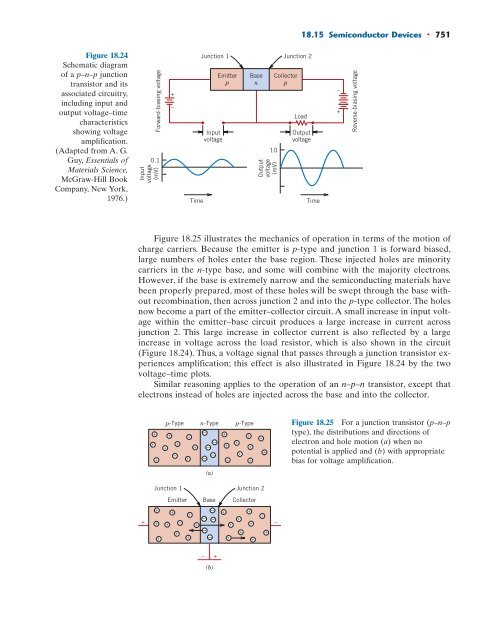
- Page 777: 18.15 Semiconductor Devices • 749
- Page 781 and 782: 18.15 Semiconductor Devices • 753
- Page 783 and 784: 18.16 Conduction in Ionic Materials
- Page 785 and 786: ands that overlap the valence and c
- Page 787 and 788: 18.19 Field Vectors and Polarizatio
- Page 789 and 790: 18.19 Field Vectors and Polarizatio
- Page 791 and 792: ionic polarization Electric dipole
- Page 793 and 794: 18.23 Dielectric Materials • 765
- Page 795 and 796: Summary • 767 + + + + + + + + +
- Page 797 and 798: Summary • 769 • With these mate
- Page 799 and 800: Summary • 771 18.11 r i Ac i 11
- Page 801 and 802: Summary • 773 One common use for
- Page 803 and 804: Questions and Problems • 775 Elec
- Page 805 and 806: Questions and Problems • 777 The
- Page 807 and 808: Design Problems • 779 DESIGN PROB
- Page 809 and 810: Chapter 19 Thermal Properties (a) (
- Page 811 and 812: 19.2 Heat Capacity • 783 Figure 1
- Page 813 and 814: 19.3 Thermal Expansion • 785 Tabl
- Page 815 and 816: 19.3 Thermal Expansion • 787 For
- Page 817 and 818: 19.4 THERMAL CONDUCTIVITY Thermal c
- Page 819 and 820: 19.4 Thermal Conductivity • 791 F
- Page 821 and 822: 19.5 Thermal Stresses • 793 speci
- Page 823 and 824: Summary • 795 • Coefficient-of-
- Page 825 and 826: Questions and Problems • 797 19.8
- Page 827 and 828: Design Problems • 799 rod be fabr
- Page 829 and 830:
WHY STUDY the Magnetic Properties o
- Page 831 and 832:
20.2 Basic Concepts • 803 I B 0 =
- Page 833 and 834:
20.3 Diamagnetism and Paramagnetism
- Page 835 and 836:
20.4 Ferromagnetism • 807 Table 2
- Page 837 and 838:
20.5 Antiferromagnetism and Ferrima
- Page 839 and 840:
20.5 Antiferromagnetism and Ferrima
- Page 841 and 842:
20.6 The Influence of Temperature o
- Page 843 and 844:
20.7 Domains and Hysteresis • 815
- Page 845 and 846:
20.7 Domains and Hysteresis • 817
- Page 847 and 848:
20.9 Soft Magnetic Materials • 81
- Page 849 and 850:
20.9 Soft Magnetic Materials • 82
- Page 851 and 852:
20.10 Hard Magnetic Materials • 8
- Page 853 and 854:
20.11 Magnetic Storage • 825 requ
- Page 855 and 856:
20.11 Magnetic Storage • 827 Figu
- Page 857 and 858:
20.12 Superconductivity • 829 Ele
- Page 859 and 860:
20.12 Superconductivity • 831 Tab
- Page 861 and 862:
Summary • 833 • For cubic ferri
- Page 863 and 864:
Questions and Problems • 835 List
- Page 865 and 866:
Questions and Problems • 837 with
- Page 867 and 868:
Design Problems • 839 H C 1T 2 H
- Page 869 and 870:
WHY STUDY the Optical Properties of
- Page 871 and 872:
21.3 Light Interactions with Solids
- Page 873 and 874:
21.4 Atomic and Electronic Interact
- Page 875 and 876:
21.5 Refraction • 847 Velocity of
- Page 877 and 878:
21.7 ABSORPTION Nonmetallic materia
- Page 879 and 880:
21.7 Absorption • 851 Reaction de
- Page 881 and 882:
21.9 Color • 853 21.9 COLOR color
- Page 883 and 884:
21.11 Luminescence • 855 Figure 2
- Page 885 and 886:
21.11 Luminescence • 857 n- and p
- Page 887 and 888:
21.13 Lasers • 859 Ruby Flash lam
- Page 889 and 890:
21.13 Lasers • 861 Partially refl
- Page 891 and 892:
21.4 Optical Fibers in Communicatio
- Page 893 and 894:
Summary • 865 Input impulse Outpu
- Page 895 and 896:
Summary • 867 Transparent nonmeta
- Page 897 and 898:
Questions and Problems • 869 Impo
- Page 899 and 900:
Design Problem • 871 fiber glass
- Page 901 and 902:
WHY STUDY Economic, Environmental,
- Page 903 and 904:
Environmental and Societal Consider
- Page 905 and 906:
Environmental and Societal Consider
- Page 907 and 908:
22.5 Recycling Issues in Materials
- Page 909 and 910:
22.5 Recycling Issues in Materials
- Page 911 and 912:
22.5 Recycling Issues in Materials
- Page 913:
Design Questions • 885 Environmen
- Page 916 and 917:
A2 • Appendix A / The Internation
- Page 918 and 919:
A4 • Appendix B / Properties of S
- Page 920 and 921:
A6 • Appendix B / Properties of S
- Page 922 and 923:
A8 • Appendix B / Properties of S
- Page 924 and 925:
A10 • Appendix B / Properties of
- Page 926 and 927:
A12 • Appendix B / Properties of
- Page 928 and 929:
A14 • Appendix B / Properties of
- Page 930 and 931:
A16 • Appendix B / Properties of
- Page 932 and 933:
A18 • Appendix B / Properties of
- Page 934 and 935:
A20 • Appendix B / Properties of
- Page 936 and 937:
A22 • Appendix B / Properties of
- Page 938 and 939:
A24 • Appendix B / Properties of
- Page 940 and 941:
A26 • Appendix B / Properties of
- Page 942 and 943:
A28 • Appendix B / Properties of
- Page 944 and 945:
A30 • Appendix B / Properties of
- Page 946 and 947:
A32 • Appendix C / Costs and Rela
- Page 948 and 949:
A34 • Appendix C / Costs and Rela
- Page 950 and 951:
Appendix D Repeat Unit Structures f
- Page 952 and 953:
A38 • Appendix D / Repeat Unit St
- Page 954 and 955:
Appendix E Glass Transition and Mel
- Page 956 and 957:
G2 • Glossary atomic mass units (
- Page 958 and 959:
G4 • Glossary according to unit c
- Page 960 and 961:
G6 • Glossary Fick’s first law.
- Page 962 and 963:
G8 • Glossary J Jominy end-quench
- Page 964 and 965:
G10 • Glossary alternating layers
- Page 966 and 967:
G12 • Glossary stock; also, elong
- Page 968 and 969:
G14 • Glossary tempered martensit
- Page 970 and 971:
Answers to Selected Problems Chapte
- Page 972 and 973:
S2 • Answers to Selected Problems
- Page 974:
S4 • Answers to Selected Problems
- Page 977 and 978:
plane strain fracture toughness, 24
- Page 979 and 980:
Clay, characteristics, 518-519 Clay
- Page 981 and 982:
Die casting, 419 Dielectric breakdo
- Page 983 and 984:
Fatigue life, 258, G4 factors that
- Page 985 and 986:
Heat treatable, definition of, 406
- Page 987 and 988:
modulus of elasticity, 486 thermal
- Page 989 and 990:
Nanotubes, carbon, 13, 471 Natural
- Page 991 and 992:
fatigue behavior (PET), 580 magneti
- Page 993 and 994:
single crystal, 451 structure of, 4
- Page 995 and 996:
Stabilized zirconia, 478, 655 Stabi
- Page 997 and 998:
Transparency, 844, G13 Transverse b
- Page 999 and 1000:
Power 1 W 0.239 cal/s 1 cal/s 4.1